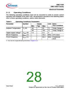
XMC1300
XMC1000 Family
Electrical Parameter
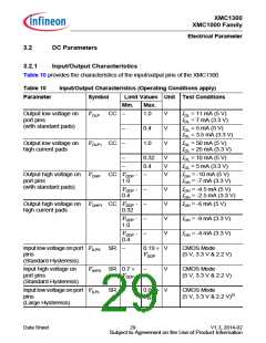
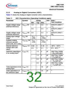
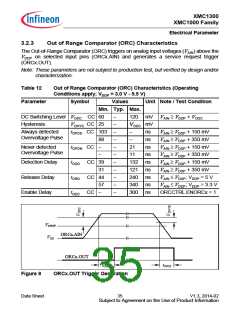
3.2.2
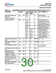
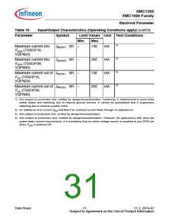
Analog to Digital Converters (ADC)
Table 11 shows the Analog to Digital Converter (ADC) characteristics.
Table 11
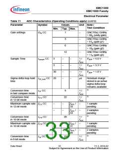
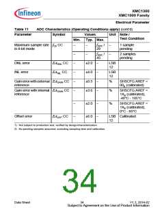
ADC Characteristics (Operating Conditions apply)
Parameter
Symbol
Values
Unit Note /
Test Condition
Min.
Typ. Max.
Supply voltage range
(internal reference)
V
DD_int SR
1.8
–
–
–
–
–
3.0
5.5
5.5
V
V
V
V
V
SHSCFG.AREF =
11B
3.0
SHSCFG.AREF =
10B
Supply voltage range
(external reference)
V
V
V
DD_ext SR 3.0
SHSCFG.AREF =
00B
Analog input voltage
range
AIN SR
VSSP
- 0.05
VDDP
+ 0.05
Auxiliary analog
REFGND SR VSSP
VDDP
reference ground
(SH0-CH0, SH1-CH0)
- 0.05
+ 0.05
Internal reference
voltage (full scale
value)
V
REFINT CC 4.82
4.9
5
5
5.18
5.1
V
V
-40°C - 105°C
0°C - 85°C 1)
Switched capacitance
of an analog input1)
C
AINS CC
–
–
–
–
–
–
1.2
1.2
4.5
4.5
–
2
pF
pF
pF
pF
pF
pF
GNCTRxz.GAINy
= 00B (unity gain)
2
GNCTRxz.GAINy
= 01B (gain g1)
6
GNCTRxz.GAINy
= 10B (gain g2)
6
GNCTRxz.GAINy
= 11B (gain g3)
1)
Total capacitance ofan CAINT CC
analog input
10
10
1)
Total capacitance of
the reference input
CAREFT CC
–
Data Sheet
32
V1.3, 2014-02
Subject to Agreement on the Use of Product Information

 INFINEON [ Infineon ]