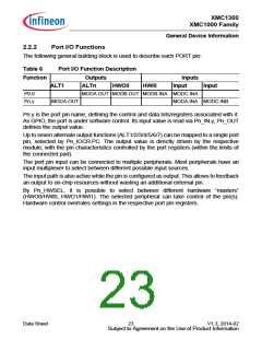
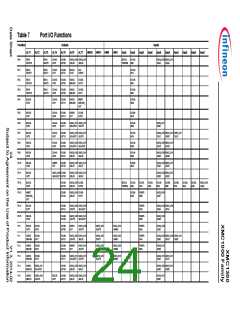
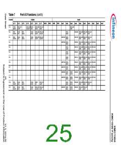
XMC1300
XMC1000 Family
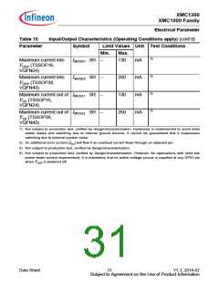
Electrical Parameter
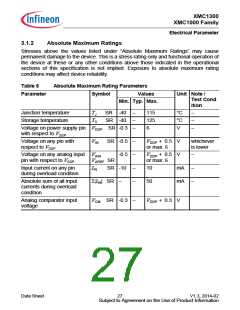
3.1.2
Absolute Maximum Ratings
Stresses above the values listed under “Absolute Maximum Ratings” may cause
permanent damage to the device. This is a stress rating only and functional operation of
the device at these or any other conditions above those indicated in the operational
sections of this specification is not implied. Exposure to absolute maximum rating
conditions may affect device reliability.
Table 8
Absolute Maximum Rating Parameters
Symbol Values
Min. Typ. Max.
Parameter
Unit Note /
Test Cond
ition
Junction temperature
Storage temperature
TJ
SR -40
SR -40
–
–
–
115
125
6
°C
°C
V
–
–
–
TS
Voltage on power supply pin VDDP SR -0.3
with respect to VSSP
Voltage on any pin with
respect to VSSP
VIN
SR -0.5
–
–
–
–
V
DDP + 0.5
V
whichever
is lower
or max. 6
Voltage on any analog input VAIN
pin with respect to VSSP
-0.5
VDDP + 0.5
V
–
–
–
VAREF SR
or max. 6
Input current on any pin
during overload condition
IIN
SR -10
10
mA
mA
Absolute sum of all input
currents during overload
condition
Σ|IIN| SR
−
50
Analog comparator input
voltage
VCM SR -0.3
–
VDDP + 0.3
V
Data Sheet
27
V1.3, 2014-02
Subject to Agreement on the Use of Product Information

 INFINEON [ Infineon ]