XMC1300
XMC1000 Family
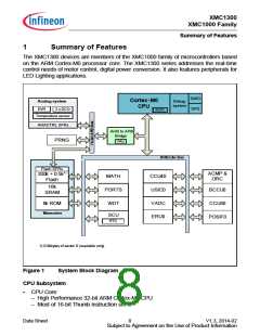
Summary of Features
Input/Output Lines With Individual Bit Controllability
•
•
•
Tri-stated in input mode
Push/pull or open drain output mode
Configurable pad hysteresis
Debug System
•
Access through the standard ARM serial wire debug (SWD) or the single pin debug
(SPD) interface
•
•
A breakpoint unit (BPU) supporting up to 4 hardware breakpoints
A watchpoint unit (DWT) supporting up to 2 watchpoints
1.1
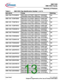
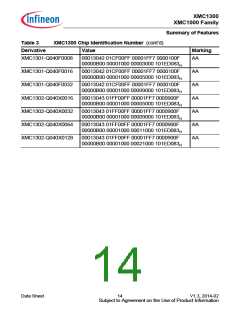
Ordering Information
The ordering code for an Infineon microcontroller provides an exact reference to a
specific product. The code “XMC1<DDD>-<Z><PPP><T><FFFF>” identifies:
•
•
<DDD> the derivatives function set
<Z> the package variant
– T: TSSOP
– Q: VQFN
•
•
<PPP> package pin count
<T> the temperature range:
– F: -40°C to 85°C
– X: -40°C to 105°C
•
<FFFF> the Flash memory size.
For ordering codes for the XMC1300 please contact your sales representative or local
distributor.
This document describes several derivatives of the XMC1300 series, some descriptions
may not apply to a specific product. Please see Table 1.
For simplicity the term XMC1300 is used for all derivatives throughout this document.
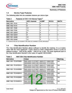
1.2
Device Types
These device types are available and can be ordered through Infineon’s direct and/or
distribution channels.
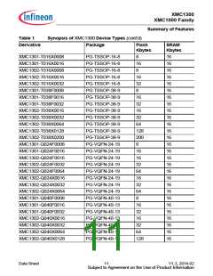
Table 1
Synopsis of XMC1300 Device Types
Derivative
Package
Flash
SRAM
Kbytes
Kbytes
XMC1301-T016F0008
XMC1301-T016F0016
PG-TSSOP-16-8
PG-TSSOP-16-8
8
16
16
16
Data Sheet
10
V1.3, 2014-02
Subject to Agreement on the Use of Product Information

 INFINEON [ Infineon ]