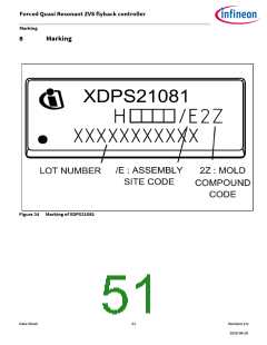
Forced Quasi Resonant ZVS flyback controller
Appendix
9
Appendix
This appendix contains additional information on electrical characteristics and specific test conditions.
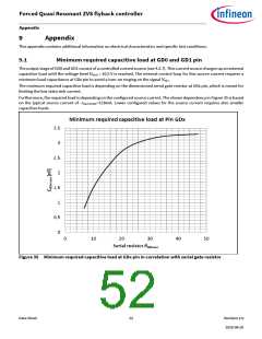
9.1
Minimum required capacitive load at GD0 and GD1 pin
The output stage of GD0 and GD1 consist of a controlled current source (see 4.2.7). This current source charges up an external
capacitive load until the voltage level VGDxH = 10.5 V is reached. The internal control loop for this source current requires a
minimum load capacitance at GDx pin to avoid a turn-on ringing on the signal VGDx
.
The minimum required capacitive load is depending on the dimensioned serial gate resistor at GDx pin, which is meant for
limiting the low state sink current.
Furthermore, the required load is depending on the configured source current. The shown dependency in Figure 35 is based
on the typical source current of –IGDxHPKSRC=118mA. Lower configured values for the source current requires also smaller
capacitive loads.
Figure 35 Minimum required capacitive load at GDx pin in correlation with serial gate resistor
Data Sheet
52
Revision 2.0
2020-08-20

 INFINEON [ Infineon ]