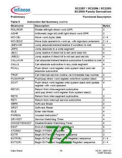
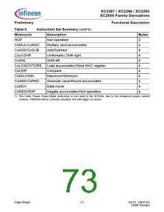
XC2287 / XC2286 / XC2285
XC2000 Family Derivatives
Preliminary
Electrical Parameters
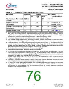
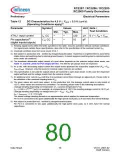
Table 10
Operating Condition Parameters (cont’d)
Parameter
Symbol
Values
Typ.
–
Unit Note /
Test Condition
Min.
Max.
5)
Absolute sum of overload Σ|IOV|
currents
–
50
mA
pF
nF
°C
External Pin Load
Capacitance
CL
–
–
–
20
680
–
–
–
–
Pin drivers in
default mode7)
Voltage Regulator Buffer CEVR
Capacitance
For each core
domain8)
Ambient temperature
TA
See Table 1
1) In case both core power domains are clocked, the difference between the power supply voltages must be less
than 10mV. This condition imposes additional constraints when using external power supplies. In order to
supply both core power domains, two independent external voltage regulators may not be used. The simplest
possibility is to supply both power domains directly via a single external power supply.
2) Performance of pad drivers, A/D Converter, and Flash module depends on VDDP
.
3) This limitation must be fulfilled under all operating conditions including power-ramp-up, power-ramp-down,
and power-save modes, if VDDI is supplied externally.
4) Overload conditions occur if the standard operating conditions are exceeded, i.e. the voltage on any pin
exceeds the specified range: VOV > VIHmax (IOV > 0) or VOV < VILmin (IOV < 0). The absolute sum of input
overload currents on all pins may not exceed 50 mA. The supply voltages must remain within the specified
limits. Proper operation under overload conditions depends on the application.
Overload conditions must not occur on pin XTAL1 (powered by VDDI).
5) Not subject to production test - verified by design/characterization.
6) An overload current (IOV) through a pin injects a certain error current (IINJ) into the adjacent pins. This error
current adds to the respective pin’s leakage current (IOZ). The amount of error current depends on the overload
current and is defined by the overload coupling factor KOV. The polarity of the injected error current is inverse
compared to the polarity of the overload current that produces it.
The total current through a pin is |ITOT| = |IOZ| + (|IOV| × KOV). The additional error current may distort the input
voltage on analog inputs.
7) The timing is valid for pin drivers operating in default current mode (selected after reset). Reducing the output
current may lead to increased delays or reduced driving capability (CL).
8) To ensure the stability of the voltage regulators each core voltage domain must be buffered with a ceramic
capacitor. For domain M a 680 nF capacitor is recommended, for domain 1 three 220 nF capacitors are
recommended. All buffer capacitors must be connected als close to the VDDI pins as possible to keep the
resistance of the board tracks below 2 Ω.
Data Sheet
74
V0.91, 2007-02
Draft Version

 INFINEON [ Infineon ]