XC2287 / XC2286 / XC2285
XC2000 Family Derivatives
Preliminary
Electrical Parameters
4
Electrical Parameters
The operating range for the XC228x is defined by its electrical parameters. For proper
operation the indicated limitations must be respected when designing a system.
Attention: The parameters and values listed in the following sections of this
Preliminary Data Sheet are preliminary and will be adjusted and
amended after the complete device characterization has been
completed.
4.1
General Parameters
These parameters are valid for all subsequent descriptions, unless otherwise noted.
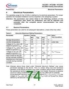
Table 9
Absolute Maximum Rating Parameters
Symbol Values
Parameter
Unit Note /
Test Condition
Min.
-65
Typ.
Max.
150
Storage temperature
Junction temperature
TST
TJ
–
–
–
°C
°C
V
–
-40
150
under bias
–
Voltage on VDDI pins with VDDIM
respect to ground (VSS)
Voltage on VDDP pins with VDDPA
,
-0.5
1.65
VDDI1
,
-0.5
-0.5
-10
–
–
–
–
–
6.0
V
–
respect to ground (VSS)
VDDPB
Voltage on any pin with
VIN
VDDP
+ 0.5
V
VIN < VDDPmax
respect to ground (VSS)
Input current on any pin
during overload condition
–
–
10
mA
mA
–
–
Absolute sum of all input
currents during overload
condition
|100|
Note: Stresses above those listed under “Absolute Maximum Ratings” may cause
permanent damage to the device. This is a stress rating only and functional
operation of the device at these or any other conditions above those indicated in
the operational sections of this specification is not implied. Exposure to absolute
maximum rating conditions for extended periods may affect device reliability.
During absolute maximum rating overload conditions (VIN > VDDP or VIN < VSS) the
voltage on VDDP pins with respect to ground (VSS) must not exceed the values
defined by the absolute maximum ratings.
Data Sheet
72
V0.91, 2007-02
Draft Version

 INFINEON [ Infineon ]