XC2287 / XC2286 / XC2285
XC2000 Family Derivatives
Preliminary
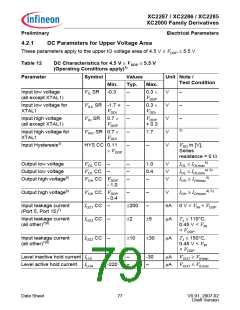
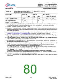
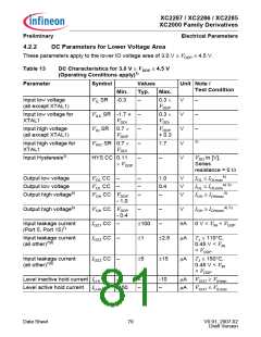
Table 12
Electrical Parameters
DC Characteristics for 4.5 V ≤ VDDP ≤ 5.5 V (cont’d)
(Operating Conditions apply)1)
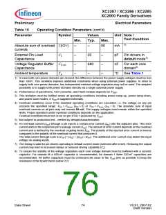
Parameter
Symbol
Values
Unit Note /
Test Condition
Min.
Typ.
Max.
±20
10
XTAL1 input current
Pin capacitance9)
IIL CC
–
–
–
–
µA 0 V < VIN < VDDI
CIO CC
pF
(digital inputs/outputs)
1) Keeping signal levels within the limits specified in this table, ensures operation without overload conditions.
For signal levels outside these specifications, also refer to the specification of the overload current IOV
.
2) Overload conditions must not occur on pin XTAL1.
3) Not subject to production test - verified by design/characterization. Hysteresis is implemented to avoid meta
stable states and switching due to internal ground bounce. It cannot suppress switching due to external system
noise under all conditions.
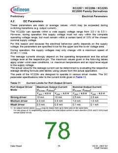
4) The maximum deliverable output current of a port driver depends on the selected output driver mode, see
Table 11, Current Limits for Port Output Drivers. The limit for pin groups must be respected.
5) As a rule, with decreasing output current the output levels approach the respective supply level (VOL→VSS,
VOH→VDDP). However, only the levels for nominal output currents are verified.
6) This specification is not valid for outputs which are switched to open drain mode. In this case the respective
output will float and the voltage results from the external circuitry.
7) An additional error current (IINJ) will flow if an overload current flows through an adjacent pin. Please refer to
the definition of the overload coupling factor KOV
.
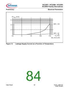
8) The given values are worst-case values. In the production test, this leakage current value is only tested at
125°C, other values are ensured via correlation. For derating, please refer to the following descriptions:
Leakage derating depending on temperature (TJ = junction temperature [°C]):
I
OZ = 0.009 × e(0.054×TJ) [µA]. For example, at a temperature of 130°C the resulting leakage current is 10.07 µA.
Leakage derating depending on voltage level (DV = VDDP - VPIN [V]):
I
OZ = IOZtempmax - (1.6 × DV) [µA]
The shown voltage derating formula is an approximation which applies for maximum temperature.
Pin P2.8 is connected to two pads (additionally the high-speed clock pad), so it sees twice the normal leakage.
9) Not subject to production test - verified by design/characterization.
Pin P2.8 is connected to two pads (additionally the high-speed clock pad), so it sees twice the normal
capacitance.
Data Sheet
78
V0.91, 2007-02
Draft Version

 INFINEON [ Infineon ]