XC2287 / XC2286 / XC2285
XC2000 Family Derivatives
Preliminary
General Device Information
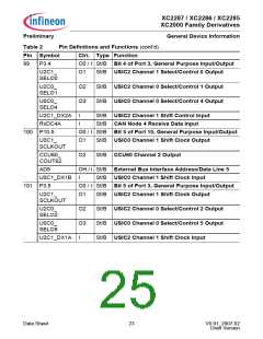
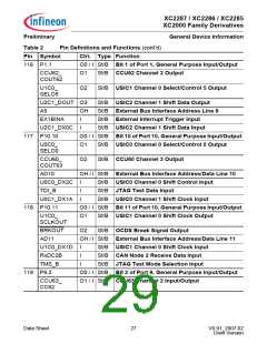
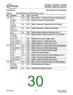
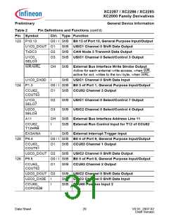
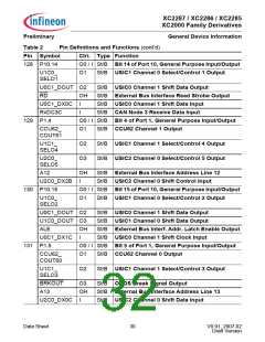
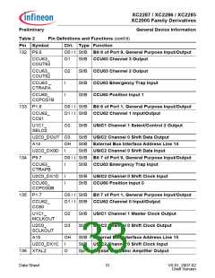
Table 2
Pin Definitions and Functions (cont’d)
Pin Symbol
116 P1.1
Ctrl. Type Function
O0 / I St/B Bit 1 of Port 1, General Purpose Input/Output
CCU62_
COUT62
O1
St/B CCU62 Channel 2 Output
U1C0_
SELO5
O2
St/B USIC1 Channel 0 Select/Control 5 Output
U2C1_DOUT O3
St/B USIC2 Channel 1 Shift Data Output
St/B External Bus Interface Address Line 9
St/B External Interrupt Trigger Input
A9
OH
I
EX1BINA
U2C1_DX0C I
117 P10.10
St/B USIC2 Channel 1 Shift Data Input
O0 / I St/B Bit 10 of Port 10, General Purpose Input/Output
U0C0_
SELO0
O1
St/B USIC0 Channel 0 Select/Control 0 Output
CCU60_
COUT63
O2
St/B CCU60 Channel 3 Output
AD10
OH / I St/B External Bus Interface Address/Data Line 10
St/B USIC0 Channel 0 Shift Control Input
U0C0_DX2C I
TDI_B
I
St/B JTAG Test Data Input
U0C1_DX1A
I
St/B USIC0 Channel 1 Shift Clock Input
118 P10.11
O0 / I St/B Bit 11 of Port 10, General Purpose Input/Output
U1C0_
O1
St/B USIC1 Channel 0 Shift Clock Output
SCLKOUT
BRKOUT
O2
St/B OCDS Break Signal Output
AD11
OH / I St/B External Bus Interface Address/Data Line 11
St/B USIC1 Channel 0 Shift Clock Input
U1C0_DX1D I
RxDC2B
TMS_B
I
St/B CAN Node 2 Receive Data Input
St/B JTAG Test Mode Selection Input
I
119 P9.2
O0 / I St/B Bit 2 of Port 9, General Purpose Input/Output
O1 / I St/B CCU63 Channel 2 Input/Output
CCU63_
CC62
Data Sheet
27
V0.91, 2007-02
Draft Version

 INFINEON [ Infineon ]