TLI4946
Specification
3.3
Operating Range
The following operating conditions must not be exceeded in order to ensure correct operation of the TLI4946xy.
All parameters specified in the following sections refer to these operating conditions unless otherwise mentioned.
Table 4
Operating Range
Parameter
Symbol
Values
Unit
Note / Test Condition
Min.
2.7
-0.7
0
Typ. Max.
Supply Voltage
Output Voltage
Output Current
VS
VQ
IQ
–
–
–
–
18
18
20
125
V
V
mA
°C
Maximum Ambient Temperature TA
-40
3.4
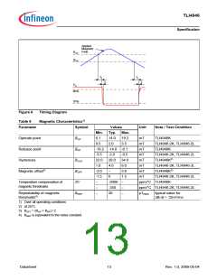
Electrical Characteristics
Product characteristics include the spread of values guaranteed within the specified voltage and ambient
temperature range. typical characteristics are the median of the production (at Vs=12V and TA=25°C).
Table 5
Parameter
Electrical Characteristics
Symbol
Values
Unit
Note / Test Condition
Min.
2
0
–
–
–
–
–
0
Typ. Max.
Supply Current
IS
4
6
mA
mA
V
µA
µs
VS=2.7 V...18 V
VS=-18 V
IQ=20 mA
VQ=18 V
RL=1.2k Ω, CL=50 pF
Reverse Current
Output Saturation Voltage
Output leakage current
Output fall time1)
Output rise time1)
Chopper frequency
Switching frequency
Delay time3)
ISR
VQSAT
IQLEAK
tf
0.2
0.3
0.05
0.02
0.4
320
–
1
0.6
10
1
1
–
152)
–
tr
µs
fOSC
fSW
td
kHz
kHz
µs
–
–
13
Output jitter4)
tQJ
1
–
µsRMS
Typical value for a 1 kHz
square wave signal
VS > 2.7 V
TLI4946K, TLI4946-2K
TLI4946-2L
Power-on Time5)
tPON
Rthja
–
–
–
13
–
µs
K/W
K/W
Thermal Resistance junction to
100
–
ambient6)
190
1) See Figure 6
2) To operate the sensor at maximum switching frequency, the value of the magnetic signal amplitude must be 1.4 times
higher than the static fields. This is due to the -3 dB corner frequency of the low pass filter in the signal path.
3) Systematic delay between magnetic threshold reached and output.
4) Jitter is the unpredictable deviation of the output switching delay.
5) Time from applying VS. > 2.7 V to the sensor until the output state is valid.
6)Relationship between junction and ambient temperature: TJ=Tamb + Rthja . (VS . IS + VQS . IQ).
Datasheet
12
Rev. 1.0, 2009-05-04

 INFINEON [ Infineon ]