TLE9879QXA40
System Control Unit - Digital Modules (SCU-DM)
•
•
•
f
f
MI_CLK; Measurement interface clock
TFILT_CLK; Analog module filter clock
LP_CLK; Clock source for all PMU submodules and WDT1
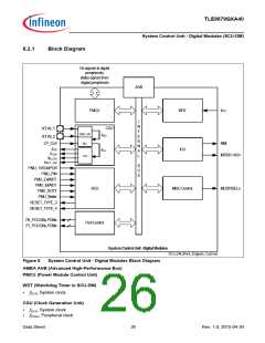
ICU (Interrupt Control Unit)
•
•
NMI (Non-Maskable Interrupt)
INTISR<15:0>; External interrupt signals
RCU (Reset Control Unit)
•
•
•
•
•
•
•
•
PMU_1V5DidPOR; Undervoltage reset of power down supply
PMU_PIN; Reset generated by reset pin
PMU_ExtWDT; WDT1 reset
PMU_IntWDT; WDT (SCU) reset
PMU_SOFT; Software reset
PMU_Wake; Sleep Mode/Stop Mode exit with reset
RESET_TYPE_3; Peripheral reset (contains all resets)
RESET_TYPE_4; Peripheral reset (without SOFT and WDT reset)
Port Control
•
•
P0_POCONy.PDMx; driver strength control
P1_POCONy.PDMx; driver strength control
MISC Control
MODPISELx; Mode selection registers for UART (source section) and Timer (trigger or count selection)
•
6.3
Clock Generation Unit
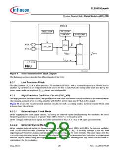
The Clock Generation Unit (CGU) enables a flexible clock generation for TLE9879QXA40. During user program
execution, the frequency can be modified to optimize the performance/power consumption ratio, allowing power
consumption to be adapted to the actual application state.
The CGU in the TLE9879QXA40 consists of one oscillator circuit (OSC_HP), a Phase-Locked Loop (PLL) module
with an internal oscillator (OSC_PLL), and a Clock Control Unit (CCU). The CGU can convert a low-frequency
input/external clock signal to a high-frequency internal clock.
The system clock fSYS is generated from of the following selectable clocks:
•
•
•
PLL clock output fPLL
Direct clock from oscillator OSC_HP fOSC
Low precision clock fLP_CLK (HW-enabled for startup after reset and during power-down wake-up sequence)
Data Sheet
27
Rev. 1.0, 2015-04-30

 INFINEON [ Infineon ]