TLE 6244X
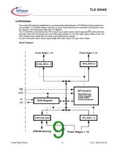
1.3 Description of the Power Stages
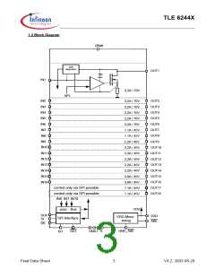
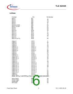
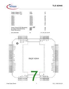
OUT1... OUT6
6 non-inverting low side power switches for nominal currents up to 2.2A. Control is possible by
input pins, by the µsec-bus or via SPI. For TJ = 25°C the on-resistance of the power switches is
below 400mΩ.
An integrated zener diode limits the output voltage to 70V typically.
A protection for inverse current is implemented for OUT1... OUT4 for use as stepper-motor con-
trol.
OUT9... OUT14
6 non-inverting low side power switches for nominal currents up to 2.2A. Control is possible by
input pins, by the µsec-bus or via SPI. For TJ = 25°C the on-resistance of the power switches is
below 380mΩ.
An integrated zener diode limits the output voltage to 45V typically.
OUT15, OUT16
2 non-inverting low side power switches for nominal currents up to 3.0A. Control is possible by
input pins, by the µsec-bus or via SPI. For TJ = 25°C the on-resistance of the power switches is
below 280mΩ.
An integrated zener diode limits the output voltage to 45V typically.
OUT7, OUT8, OUT17, OUT18
4 low side power switches for nominal currents up to 1100mA. Stage 7 is non-inverting, Stage 8
is inverting (IN8 = ‘1’ => OUT8 is active). For the output OUT7 control is possible by the input pin,
by the µsec-bus or via SPI, OUT8 is controlled by the input pin IN8 or via SPI, for the outputs
OUT17 and OUT18 control is only possible via SPI. For TJ = 25°C the on-resistance of the power
switches is below 780mΩ.
An integrated zener diode limits the output voltage to 45V typically.
In order to increase the switching current or to reduce the power dissipation parallel connection
of power stages is possible (for additional information see 1.13).
The power stages are short-circuit proof:
Power stages OUT1...OUT8, OUT11.14: In case of overload (SCB) they will be turned off after a
given delay time. During this delay time the output current is limited by an internal current control
loop.
Power stages OUT9, OUT10, OUT15...OUT18:
In case of SCB these power stages can be configured for a shut-down mode or for static current
limitation. In the shut down mode while SCB they will behave like OUT1..8 or OUT11..14.
In case of static current limitation and SCB the current is limited and the corresponding bit com-
bination is set (early warning) after a given delay time. They will not be turned off. If this condition
leads to an overtemperature condition, the output will be set into a low duty cycle PWM (selective
thermal shut- down with restart) to prevent critical chip temperature.
There are 3 possibilities to turn the power stages on again:
- turn the power stage off and on, either via serial control (SPI) or via parallel control (input pin,
except outputs OUT17 and OUT18) or by the µsec-bus (except OUT8, OUT17,OUT18)
- applying a reset signal.
- sending the instruction “del_dia” by the SPI-interface
The VDD-monitoring locks all power stages, except OUT8 for access by the IN8 input. OUT8 is
locked by an internal threshold of 3,5V maximum when controlled by IN8. Otherwise OUT8 is
locked by the VDD-monitor.
Final Data Sheet
4
V4.2, 2003-08-29

 INFINEON [ Infineon ]