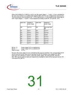
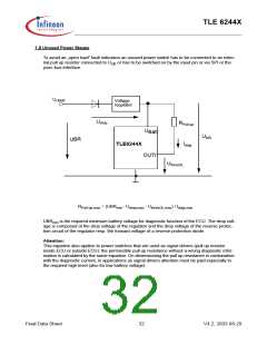
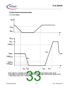
TLE 6244X
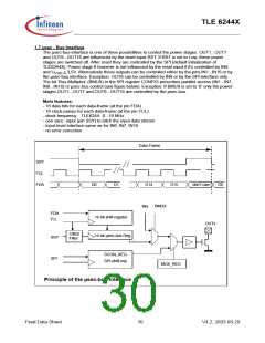
1.7 µsec - Bus Interface
The µsec-bus-interface is one of three possibilities to control the power stages. OUT1...OUT7
and OUT9...OUT16 are influenced by the reset input RST. If RST is set to Low, these power
stages are switched off. After reset they are controlled by the SPI (default initialization of
TLE6244X). Power stage 8 however is not influenced by the reset input if it’s controlled by IN8
and UVDD > 3,5V. Alternatively these outputs can be controlled either by the pins IN1...IN16 or by
the µsec-bus interface. Exception: OUT8 can be controlled by IN8 or by the SPI-interface only.
The bit ’Bus-Multiplex’ (BMUX) in the SPI register CONFIG prescribes parallel access (IN1...IN7,
IN9...IN16) or µsec-bus control (see figure below). Exception: If BMUX is set to ‘0’ only the power-
stages OUT1...OUT7 and OUT9...OUT16 are controlled by the µsec-bus.
Main features:
- 16 data bits for each data-frame (at the pin FDA)
- 16 clock-pulses for each data-frame (at the pin FCL)
- clock frequency TLE6244: 0...16 MHz
- one sync -input (pin SSY) to latch the input data stream
- input level interface same as for IN6, IN7, IN16
- no error correction
Data-Frame
SSY
FCL
FDA
D0
D1
D14
D15
don’t care
D0
BMUX
INx
FDA
FCL
16 bit shift register
OUTx
Glitch
Filter
16 bit µsec-bus Reg.
SSY
SPI
SCON_REG
SPI-shift-reg
MUX_REG
Principle of the µsec-bus interface
Final Data Sheet
30
V4.2, 2003-08-29

 INFINEON [ Infineon ]