TDA5235
Functional Description
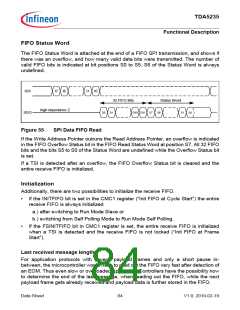
Therefore the last received message length (e.g. after an EOM event) is stored in
register PLDLEN and the upper two bits of register RFPLLACC at TSI detection of the
next message. The upper two bits of register RFPLLACC hold the MSBs, thus a
message length of 256 up to 1023 payload bits can be depicted. A saturation of the
message length at the maximum value of 1023 is realized. Storage at TSI of the next
message ensures that even wrong payload data (e.g. if MID is not matching, no EOM
will be generated, but payload is kept in FIFO. Or EOM data length criterion is selected
only and a sync loss prevents from generating an EOM event) can be identified.
On initialization of the FIFO, the register PLDLEN and the upper two bits of register
RFPLLACC are cleared. The corresponding internal counter is cleared with every TSI
detection and initialization of the FIFO.
PLDLEN will work correctly in case:
(INITDRXES = 0) AND ( (Data rate > 22kBit/s) OR (EOM2SPM = 0) )
If the condition above is not fulfilled, then the chip internal state machine can set
PLDLEN to 0 and a correct function of PLDLEN cannot be guaranteed.
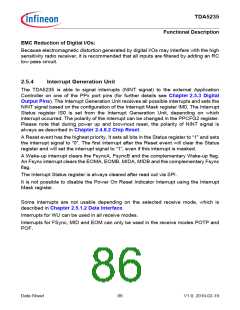
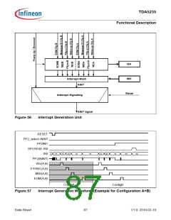
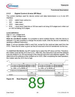
2.5.3
Digital Output Pins
As long as the P_ON pin is high, all digital output pins operate as described. If the P_ON
pin is low, all digital output pins are switched to high impedance mode.
The digital outputs PP0, PP1, PP2 and PP3 are configurable, where each of the signals
CLK_OUT, RX_RUN, NINT, a LOW level (GND) and a HIGH level, DATA,
DATA_MATCHFIL, CH_DATA, CH_STR, RXD and RXSTR can be routed to any of the
four output pins. There is only one exception, CLK_OUT is not available on PP3. The
default configuration for these four output pins can be seen in Table 1.
Each port pin can be inverted by usage of PPCFG2 register.
The RX_RUN signal is active high for all Configurations by default. It can be deactivated
for every Configuration separately. Every PPx can be configured with an individual
RX_RUN setup. This can be set in RXRUNCFG0 and RXRUNCFG1 registers.
Interfacing to 3.3V Logic:
The TDA5235 is able to interface directly to a 3.3V logic, when chip is operated in 3.3V
environment.
Interfacing to 5V Logic:
The TDA5235 is able to interface directly to a 5V logic, when chip is operated in 5V
environment.
Data Sheet
85
V1.0, 2010-02-19

 INFINEON [ Infineon ]