TDA5235
Functional Description
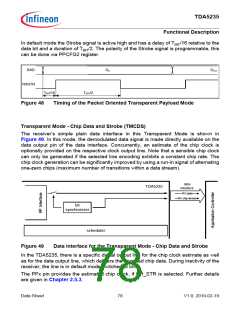
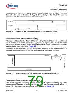
2.5.2
Receive FIFO
The Receive FIFO is the storage of the received data frames and is only used in the POF
Mode. It is written during data reception. The host microcontroller is able to start reading
via SPI right after frame sync (interrupt) or in the most common case right after detection
of EOM (interrupt). The FIFO can store up to 256 received data bits. If the expected data
transmission contains more bits (note that in TSI 8-bit Extended Mode one bit is added
in front of the real payload to indicate which of the two TSI pattern has matched), reading
from FIFO must start a certain time after frame sync to prevent an overrun.
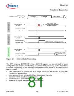
Architecture
The 256-bit receive FIFO is based on a bit-addressable 2-port memory architecture.
Data
from
Digital-
Receiver
Write-Port
Write Address
Pointer
(Up-Counter)
Bit-Address
In
1 of 16 Decoder
Data Clock
ENABLE
RESET
byte
byte
byte
byte
byte
byte
byte
byte
byte
0
1
2
3
4
5
6
7
8
byte 16
byte 17
byte 18
byte 19
byte 20
byte 21
byte 22
byte 23
byte 24
256-bit
Memory-Array
byte
9
byte 25
byte 26
byte 27
byte 28
byte 29
byte 30
byte 31
byte 10
byte 11
byte 12
byte 13
byte 14
byte 15
from FSM
INITFIFO
Read Address
Pointer
(Up-Counter)
FSINITFIFO
InitFIFO
16 to 1 MUX
Out
Bit-Address
Read-Port
SCLK
RESET
ENABLE
to
SPI-Bus
FIFO-Overflow
# of Valid Bits
from FSync
Digital-
FIFO-
Controller
EOM
SDO
Receiver
SDO-Frame
Generator
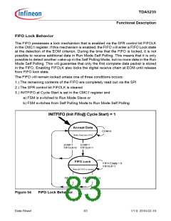
FIFOLK
fifolk
to FSM
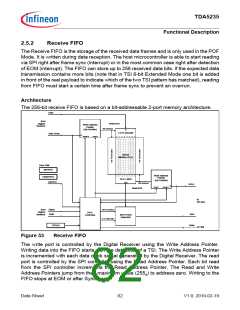
Figure 53
Receive FIFO
The write port is controlled by the Digital Receiver using the Write Address Pointer.
Writing data into the FIFO starts with the detection of a TSI. The Write Address Pointer
is incremented with each data clock signal generated by the Digital Receiver. The read
port is controlled by the SPI controller using the Read Address Pointer. Each bit read
from the SPI controller increments the Read Address Pointer. The Read and Write
Address Pointers jump from their maximum value (255d) to address zero. Writing to the
FIFO stops at EOM or after Sync loss.
Data Sheet
82
V1.0, 2010-02-19

 INFINEON [ Infineon ]