TDA5235
Functional Description
2.4.8
Digital Baseband (DBB) Receiver
Blind Sync
Initial Phase & Data rate
CDR PLL
FSK
detector
CR PLL
Slicer
sync
chip_data_clock
CH_STR
adjust_length
SRC
bypass
8 to 16
samples
per chip
Matched Filter
Chip
Data
Invert
chip_data
Signal
Detector
Data
Slicer
Chip Data
Decoder
CH_DATA
fractional SRC
From ASK/
FSK
fsout / fsin = 0.5 … 1.0
Demodulator
CHIPDINV
Decoder
MUX
RAW Data Slicer
for external
processing
data_clk
data
SIGN
Data
eom
FIFO
Framer
(TSI Detector)
fsync
wakeup
WU Unit
Data
Invert
DINVEXT
Invert
RXSTR RXD
DATA
(Sliced RAW Data for
external processing)
DATA_MATCHFIL
(Matched Filtered Data
for external processing )
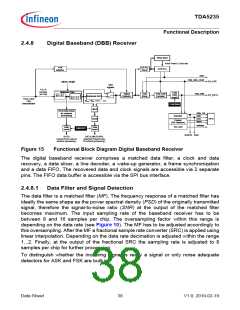
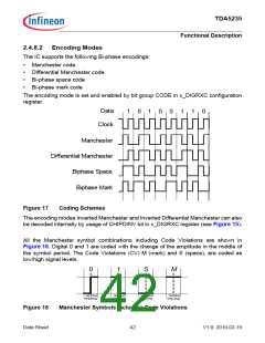
Figure 15
Functional Block Diagram Digital Baseband Receiver
The digital baseband receiver comprises a matched data filter, a clock and data
recovery, a data slicer, a line decoder, a wake-up generator, a frame synchronization
and a data FIFO. The recovered data and clock signals are accessible via 2 separate
pins. The FIFO data buffer is accessible via the SPI bus interface.
2.4.8.1 Data Filter and Signal Detection
The data filter is a matched filter (MF). The frequency response of a matched filter has
ideally the same shape as the power spectral density (PSD) of the originally transmitted
signal, therefore the signal-to-noise ratio (SNR) at the output of the matched filter
becomes maximum. The input sampling rate of the baseband receiver has to be
between 8 and 16 samples per chip. The oversampling factor within this range is
depending on the data rate (see Figure 10). The MF has to be adjusted accordingly to
this oversampling. After the MF a fractional sample rate converter (SRC) is applied using
linear interpolation. Depending on the data rate decimation is adjusted within the range
1...2. Finally, at the output of the fractional SRC the sampling rate is adjusted to 8
samples per chip for further processing.
To distinguish whether the incoming signal is really a signal or only noise adequate
detectors for ASK and FSK are built in.
Data Sheet
38
V1.0, 2010-02-19

 INFINEON [ Infineon ]