TDA5235
Appendix
Register Overview
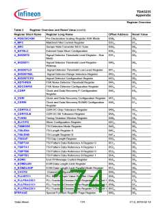
Table 2
Register Overview and Reset Value (cont’d)
Register Short Name
B_EXTSLC
Register Long Name
Offset Address Reset Value
Externel Data Slicer Configuration
13EH
13FH
02H
00H
B_SIGDET0
Signal Detector Threshold Level Register - Run
Mode
B_SIGDET1
Signal Detector Threshold Level Register -
Wakeup
140H
00H
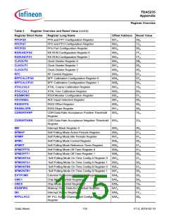
B_SIGDETLO
B_SIGDETSEL
B_SIGDETCFG
B_NDTHRES
B_NDCONFIG
B_CDRP
Signal Detector Threshold Low Level Register
Signal Detector Range Selection Register
Signal Detector Configuration Register
FSK Noise Detector Threshold Register
FSK Noise Detector Configuration Register
141H
142H
143H
144H
145H
146H
00H
7FH
00H
00H
07H
E6H
Clock and Data Recovery P Configuration
Register
B_CDRI
Clock and Data Recovery Configuration Register 147H
65H
01H
B_CDRRI
Clock and Data Recovery RUNIN Configuration
Register
148H
B_CDRTOLC
B_CDRTOLB
B_TVWIN
CDR DC Chip Tolerance Register
CDR DC Bit Tolerance Register
Timing Violation Window Register
Slicer Configuration Register
149H
14AH
14BH
14CH
14DH
14EH
14FH
150H
151H
152H
153H
154H
155H
156H
157H
158H
159H
0CH
1EH
28H
90H
80H
00H
00H
00H
00H
00H
00H
00H
05H
00H
00H
04H
93H
F3H
07H
09H
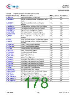
B_SLCCFG
B_TSIMODE
B_TSILENA
B_TSILENB
B_TSIGAP
TSI Detection Mode Register
TSI Length Register A
TSI Length Register B
TSI Gap Length Register
B_TSIPTA0
B_TSIPTA1
B_TSIPTB0
B_TSIPTB1
B_EOMC
TSI Pattern Data Reference A Register 0
TSI Pattern Data Reference A Register 1
TSI Pattern Data Reference B Register 0
TSI Pattern Data Reference B Register 1
End Of Message Control Register
EOM Data Length Limit Register
EOM Data Length Limit Parallel Mode Register
Channel Configuration Register
PLL MMD Integer Value Register Channel 1
B_EOMDLEN
B_EOMDLENP
B_CHCFG
B_PLLINTC1
B_PLLFRAC0C1
B_PLLFRAC1C1
B_PLLFRAC2C1
PLL Fractional Division Ratio Register 0 Channel 1 15AH
PLL Fractional Division Ratio Register 1 Channel 1 15BH
PLL Fractional Division Ratio Register 2 Channel 1 15CH
Data Sheet
178
V1.0, 2010-02-19

 INFINEON [ Infineon ]