TDA 5210
Applications
3
2.5
2
RSSI Level
1.5
1
0.5
0
-120
-110
-100
-90
-80
-70
-60
-50
-40
-30
Input Level at LNA Input [dBm]
RSSI-AGC.wmf
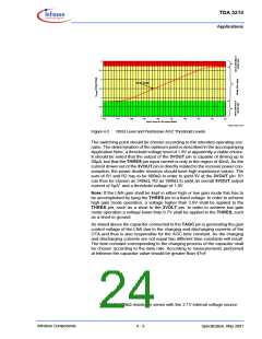
Figure 4-2
RSSI Level and Permissive AGC Threshold Levels
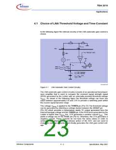
The switching point should be chosen according to the intended operating sce-
nario. The determination of the optimum point is described in the accompanying
Application Note, a threshold voltage level of 1.8V is apparently a viable choice.
It should be noted that the output of the 3VOUT pin is capable of driving up to
50µA, but that the THRES pin input current is only in the region of 40nA. As the
current drawn out of the 3VOUT pin is directly related to the receiver power con-
sumption, the power divider resistors should have high impedance values. The
sum of R1 and R2 has to be 600kΩ in order to yield 3V at the 3VOUT pin. R1
can thus be chosen as 240kΩ, R2 as 360kΩ to yield an overall 3VOUT output
current of 5µA1 and a threshold voltage of 1.8V
Note: If the LNA gain shall be kept in either high or low gain mode this has to
be accomplished by tying the THRES pin to a fixed voltage. In order to achieve
high gain mode operation, a voltage higher than 2.8V shall be applied to the
THRES pin, such as a short to the 3VOLT pin. In order to achieve low gain
mode operation a voltage lower than 0.7V shall be applied to the THRES, such
as a short to ground.
As stated above the capacitor connected to the TAGC pin is generating the gain
control voltage of the LNA due to the charging and discharging currents of the
OTA and thus is also responsible for the AGC time constant. As the charging
and discharging currents are not equal two different time constants will result.
The time constant corresponding to the charging process of the capacitor shall
be chosen according to the data rate. According to measurements performed
at Infineon the capacitor value should be greater than 47nF.
1. note the 20kΩ resistor in series with the 3.1V internal voltage source
Wireless Components
4 - 3
Specification, May 2001

 INFINEON [ Infineon ]