TC1796
Electrical Parameters
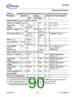
Table 12
Parameter
Operating Condition Parameters
Symbol Values
Typ. Max.
Unit Note /
Test Condition
Min.
Σ|ISC| SR –
Absolute sum of short
circuit currents of the
device
–
100
mA See note10)
External load
capacitance
CL
SR –
–
–
pF
Depending on pin
class. See DC
characteristics
1) Digital supply voltages applied to the TC1796 must be static regulated voltages which allow a typical voltage
swing of ±5%.
2) VDDOSC and VSSOSC are not bonded externally in the BC and BD steps of TC1796. An option for bonding them
in future steps and products is kept open.
3) Voltage overshoot up to 1.7 V is permissible at Power-Up and PORST low, provided the pulse duration is less
than 100 µs and the cumulated summary of the pulses does not exceed 1 h.
4) Voltage overshoot to 4 V is permissible at Power-Up and PORST low, provided the pulse duration is less than
100 µs and the cumulated summary of the pulses does not exceed 1 h
5) The VDDSB must be properly connected and supplied with power. If not, the TC1796 will not operate. In case
of a stand-by operation, the core voltage must not float, but must be pulled low, in order to avoid internal cross-
currents.
6) This applies only during power down state. During normal SRAM operation regular VDD has to be applied.
7) The TC1796 uses a static design, so the minimum operation frequency is 0 MHz. Due to test time restriction
no lower frequency boundary is tested, however.
8) The PLL jitter characteristics add to this value according to the application settings. See the PLL jitter
parameters.
9) Applicable for digital outputs.
10) See additional document “TC1796 Pin Reliability in Overload“ for overload current definitions.
Table 13
Group
Pin Groups for Overload/Short-Circuit Current Sum Parameter
Pins
1
2
3
4
5
6
7
8
P4.[7:0]
P4.[14:8]
P4.15, SLSO[1:0], SCLK0, MTSR0, MRST0, SLSI0
WAIT, HOLD, BC[3:0], HLDA, MR/W, BAA, CSCOMB
CS[3:0], RD, RD/WR, BREQ, ADV, BFCLKO
BFCLKI, D[31:24]
D[23:16]
D[15:8]
Data Sheet
86
V1.0, 2008-04

 INFINEON [ Infineon ]