TC1796
Electrical Parameters
4.1.4
Operating Conditions
The following operating conditions must not be exceeded in order to ensure correct
operation of the TC1796. All parameters specified in the following table refer to these
operating conditions, unless otherwise noticed.
The following operating conditions must not be exceeded in order to ensure correct
operation of the TC1796. All parameters specified in the following table refer to these
operating conditions, unless otherwise noted.
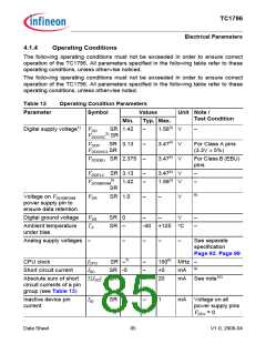
Table 12
Parameter
Operating Condition Parameters
Symbol Values
Typ. Max.
Unit Note /
Test Condition
Min.
Digital supply voltage1) VDD
SR 1.42
–
1.583)
3.474)
3.474)
V
V
V
–
VDDOSC2) SR
VDDP
SR 3.13
DDOSC3 SR
VDDEBU SR 2.375 –
–
For Class A pins
(3.3V ± 5%)
For Class B (EBU)
pins
V
VDDFL3 SR 3.13
–
–
3.474)
1.583)
V
V
–
–
5)
VDDSBRAM
1.42
SR
SR 1.0
6)
Voltage on VDDSBRAM
power supply pin to
ensure data retention
VDR
–
–
V
Digital ground voltage
Ambient temperature
under bias
VSS
TA
SR 0
SR –
–
–
V
–
–
-40 +125 °C
Analog supply voltages –
–
–
–
–
See separate
specification
Page 92, Page 99
CPU clock
Short circuit current
fCPU
ISC
SR –7)
SR -5
–
–
–
1508) MHz –
+5
20
9)
mA
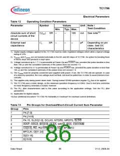
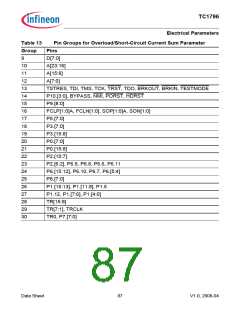
Absolute sum of short
circuit currents of a pin
group (see Table 13)
Σ|ISC| SR –
mA See note10)
Inactive device pin
current
IID
SR -1
–
1
mA Voltage on all
power supply pins
V
DDx = 0
Data Sheet
85
V1.0, 2008-04

 INFINEON [ Infineon ]