TC1796
Summary of Features
– One MultiCAN Module with four CAN nodes and 128 free assignable message
objects for high efficiency data handling via FIFO buffering and gateway data
transfer (one CAN node supports TTCAN functionality)
– Two General Purpose Timer Array Modules (GPTA) with additional Local Timer
Cell Array (LTCA2) providing a powerful set of digital signal filtering and timer
functionality to realize autonomous and complex Input/Output management
– Two 16-channel Analog-to-Digital Converter units (ADC) with selectable 8-bit, 10-
bit, or 12-bit resolution
– One 4-channel Fast Analog-to-Digital Converter unit (FADC) with concatenated
comb filters for hardware data reduction: supporting 10-bit resolution, min.
conversion time of 280ns
•
•
•
•
•
44 analog input lines for ADC and FADC
123 digital general purpose I/O lines, 4 input lines
Digital I/O ports with 3.3 V capability
On-chip debug support for OCDS Level 1 and 2 (CPU, PCP3, DMA)
Dedicated Emulation Device chip for multi-core debugging, tracing, and calibration
via USB V1.1 interface available (TC1796ED)
•
•
•
•
•
•
Power Management System
Clock Generation Unit with PLL
Core supply voltage of 1.5 V
I/O voltage of 3.3 V
Full automotive temperature range: -40° to +125°C
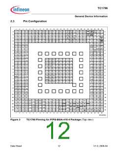
P/PG-BGA-416-4 package
Data Sheet
8
V1.0, 2008-04

 INFINEON [ Infineon ]