TC1767
Pinning
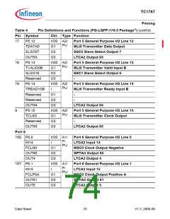
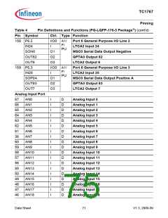
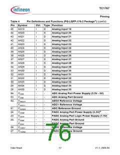
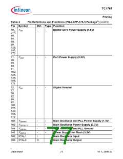
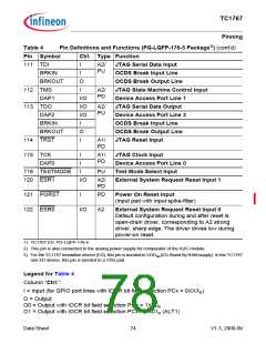
Table 4
Pin Definitions and Functions (PG-LQFP-176-5 Package1)) (cont’d)
Ctrl. Type Function
Pin Symbol
111 TDI
BRKIN
I
A2/
PU
JTAG Serial Data Input
OCDS Break Input Line
OCDS Break Output Line
JTAG State Machine Control Input
Device Access Port Line 1
JTAG Serial Data Output
Device Access Port Line 2
OCDS Break Input Line
OCDS Break Output Line
JTAG Reset Input
I
BRKOUT
112 TMS
DAP1
O
I
A2/
PD
I/O
I/O
I/O
I
113 TDO
DAP2
A2/
PU
BRKIN
BRKOUT
114 TRST
O
I
A1/
PD
115 TCK
DAP0
I
A1/
PD
JTAG Clock Input
I
Device Access Port Line 0
Test Mode Select Input
118 TESTMODE
120 ESR1
I
PU
I/O
A2/
PD
External System Request Reset Input 1
121 PORST
122 ESR0
I
PD
Power On Reset Input
(input pad with input spike-filter)
I/O
A2
External System Request Reset Input 0
Default configuration during and after reset is
open-drain driver, corresponding to A2 strong
driver, sharp edge. The driver drives low during
power-on reset.
1) TC1767 ED: PG-LQFP-176-6
2) This pin is also connected to the analog power supply for comparator of the ADC module.
3) For the TC1767 emulation device (ED), this pin is bonded to VDDSB (ED Stand By RAM supply). In the TC1767
non ED device, this pin is bonded to a VDD pad.
Legend for Table 4
Column “Ctrl.”:
I = Input (for GPIO port lines with IOCR bit field selection PCx = 0XXXB)
O = Output
O0 = Output with IOCR bit field selection PCx = 1X00B
O1 = Output with IOCR bit field selection PCx = 1X01B (ALT1)
Data Sheet
74
V1.3, 2009-09

 INFINEON [ Infineon ]