PEB 2091
PEF 2091
Electrical Characteristics
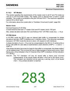
8.7.6.2 NT Modes
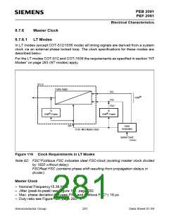
This section specifies the requirements of the master clock in all NT and TE modes as
well as in COT-512/1536 modes. The master clock is derived from a built-in crystal
oscillator. The crystal is connected to the pins XIN and XOUT. The maximum capacitive
load at XIN is 40 pF each.
For information about the crystal refer to "Oscillator Circuit and Crystal", page 252.
Master Clock
Nominal frequency15.36 MHz
Overall tolerance between LT master clock and NT master clock± 100 ppm
Max. phase deviation between FSC and fictitious FSC* (NT-PBX mode only) : ± 18 µs
NT-PBX Mode
In NT-PBX mode the IEC-Q uses an internal data buffer to compensate for phase
deviations between IOM®-2-interface and U-interface clocks. This becomes necessary
because in NT-PBX mode the device is slave with respect to both interfaces.
A phase deviation of up to ± 18 µs can be compensated by the IEC-Q. To achieve this a
64 bit wide buffer for user data is implemented in each direction (IOM®-2 → U and U →
IOM®-2).
If the phase deviation becomes too large for the buffer to compensate, the phase relation
will be redetermined. This involves the loss of data because a frame jump occurs. Each
frame jump will be indicated in the C/I Channel of the IOM®-2-interface with the indication
"FJ" (0010B).
Note 83: The "FJ" indication will only be issued after a frame jump occurred
(independently of the actual phase deviation which led to the frame jump).
This indication can therefore not be used as a warning which will be issued
when ± 18 µs phase deviation is reached.
Semiconductor Group
283
Data Sheet 01.99

 INFINEON [ Infineon ]