PEB 2091
PEF 2091
Electrical Characteristics
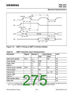
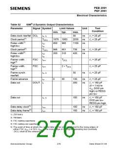
Table 52
IOM®-2 Dynamic Output Characteristics
Signal Symbol Limit Values
Parameter
Unit
Test
Condition
min. typ.
max.
Data clock rise/fall DCL
Clock period1)
Pulse width1)
high/low
tR, tF
30
ns
ns
ns
CL = 25 pF
CL = 25 pF
TDCL
1875 1953
2035
1105
twH
twL
850
960
Clock period2)
Pulse width2)
high/low
TDCL
565
200
651
310
735
420
ns
ns
CL = 25 pF
twH
twL
Frame width
high3)
FSC
FSC
twFH
twFH
tR, tF
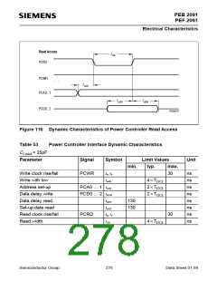
tdF
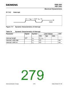
TDCL
CL = 25 pF
CL = 25 pF
CL = 25 pF
CL = 25 pF
Frame width
high4)
2 × TDCL
Frame synch.
rise/fall
30
ns
Frame advance
Data out
0
65
130
200
ns
ns
DOUT tF
CL = 150 pF
(R = 1 kΩ to
VDD, DOD pin
high) or RESQ
pin low
Data out
tR, tF
150
ns
CL = 150 pF
DOD pin low
RESQ pin high
Data delay clock5)
Data delay frame5)
tdDC
tdDF
100
150
ns
ns
CL = 150 pF
CL = 150 pF
1) 256 kbit/s
2) 768 kbit/s
3) FSC marking superframe
4) FSC marking non-superframe
5) The point of time at which the output data will be valid is referred to the rising edges of
either FSC (tdDF ) or DCL (tdDC ). The rising edge of the signal appearing last (normally
DCL) shall be the reference
Semiconductor Group
276
Data Sheet 01.99

 INFINEON [ Infineon ]