PEB 2091
PEF 2091
Electrical Characteristics
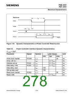
Table 50
= 50pF
Timing Characteristics (serial µP interface mode)
C
Load
Parameter
Symbol
tP
min. max. unit
Clock period
130
0
ns
ns
ns
ns
ns
ns
Chip Select setup time
Chip Select hold time
CDIN setup time
CDIN hold time
tCSs
tCSh
20
40
40
tCDINs
tCDINh
tCDOUTd
CDOUT data out delay
30
®
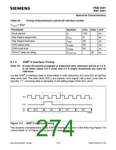
8.7.3
IOM -2 Interface Timing
Note 79: In case the period of signals is stated the time reference will be at 1.4 V;
in all other cases 0.8 V (low) and 2.0 V (high) thresholds are used as
reference.
Via the IOM®-2-interface data is transmitted in both directions (DU and DD) at half the
data clock rate. The data clock (DCL) is a square wave signal with a duty cycle ratio of
typically 1:1. Incoming data is sampled on the falling edge of the DCL-clock.
"a"
DCL
FSC
DU
Bit 32
Bit 0
Bit 1
Bit 2
DD
ITD04228
Figure 113 IOM®-2 Interface Timing
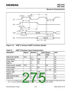
The dynamic characteristics of the IOM®-2-interface is given in the following Figure 114
where Detail "a" of Figure 113 is shown in more detail.
Semiconductor Group
274
Data Sheet 01.99

 INFINEON [ Infineon ]