PEB 2091
PEF 2091
Electrical Characteristics
Pin Capacitances
TA = 25 °C; VDD = 5 V ± 5 %; VSS = 0 V; fC = 1 MHz
Pin
Symbol
Limit Values
Unit
min.
max.
DIN, PS1, PS2, DCL (input), FSC CIO
10
pF
(input), DOUT (open)
XIN, XOUT
CIO
CIO
5
7
pF
pF
All other pins
8.7
AC Characteristics
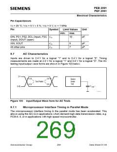
Inputs are driven to 2.4 V for a logical "1" and to 0.4 V for a logical "0". Timing
measurements are made at 2.0 V for a logical "1" and 0.8 V for a logical "0". The AC
testing input/output wave forms are shown in Figure 103 below.
2.4
2.0
0.8
2.0
0.8
Device
Under
Test
Test Points
C Load = 150 pF
0.45
ITS00621
Figure 103 Input/Output Wave form for AC Tests
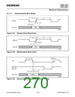
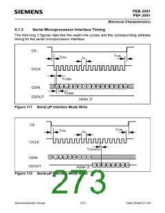
8.7.1
Microprocessor Interface Timing in Parallel Mode
The microprocessor interface timing in the parallel mode has been accelerated. This
allows using the IEC-Q in applications which demand high data transmission rates, e.g.
PCM-4, 8, or in applications with high speed microcontroller.
Semiconductor Group
269
Data Sheet 01.99

 INFINEON [ Infineon ]