IRFS7434-7PPbF
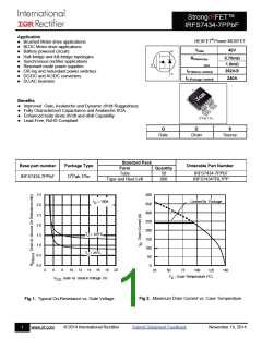
Dynamic Electrical Characteristics @ TJ = 25°C (unless otherwise specified)
Symbol
gfs
Parameter
Forward Transconductance
Total Gate Charge
Min. Typ. Max. Units
Conditions
VDS = 10V, ID =100A
ID = 100A
156 –––
––– 210
––– 55
––– 66
––– 144
––– 23
––– 125
–––
315
–––
–––
–––
–––
–––
S
Qg
Qgs
Gate-to-Source Charge
Gate-to-Drain Charge
Total Gate Charge Sync. (Qg– Qgd)
Turn-On Delay Time
VDS = 20V
nC
Qgd
VGS = 10V
Qsync
td(on)
tr
VDD = 26V
ID = 100A
Rise Time
ns
td(off)
tf
Turn-Off Delay Time
Fall Time
––– 107
––– 85
–––
–––
RG= 2.6
VGS = 10V
Ciss
Coss
Crss
Input Capacitance
Output Capacitance
Reverse Transfer Capacitance
––– 10250 –––
––– 1540 –––
––– 1060 –––
VGS = 0V
VDS = 25V
ƒ = 1.0MHz, See Fig.7
pF
VGS = 0V, VDS = 0V to 32V
Coss eff.(ER) Effective Output Capacitance (Energy Related) ––– 1880 –––
See Fig.11
Coss eff.(TR) Output Capacitance (Time Related)
––– 2147 –––
VGS = 0V, VDS = 0V to 32V
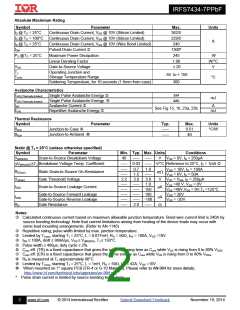
Diode Characteristics
Symbol
IS
Parameter
Continuous Source Current
(Body Diode)
Pulsed Source Current
(Body Diode)
Min. Typ. Max. Units
Conditions
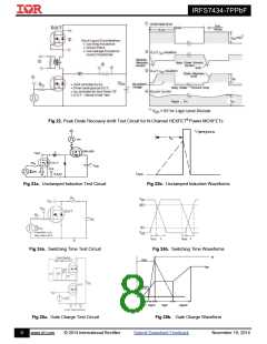
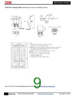
MOSFET symbol
D
––– ––– 362
A
––– ––– 1300*
showing the
G
integral reverse
p-n junction diode.
ISM
S
VSD
Diode Forward Voltage
––– 0.9
1.3
V
TJ = 25°C,IS = 100A,VGS = 0V
dv/dt
Peak Diode Recovery dv/dt
––– 3.0
––– 44
––– 46
––– 43
––– 44
––– 1.9
––– V/ns TJ = 150°C,IS =100A,VDS = 40V
–––
–––
–––
–––
–––
TJ = 25°C
VDD = 34V
IF = 100A,
trr
Reverse Recovery Time
ns
TJ = 125°C
TJ = 25°C di/dt = 100A/µs
Qrr
Reverse Recovery Charge
Reverse Recovery Current
nC
A
TJ = 125°C
IRRM
TJ = 25°C
3
www.irf.com
© 2014 International Rectifier
Submit Datasheet Feedback
November 19, 2014

 INFINEON [ Infineon ]