IRFS7434-7PPbF
Absolute Maximium Rating
Symbol
Parameter
Max.
362
229
Units
ID @ TC = 25°C
Continuous Drain Current, VGS @ 10V (Silicon Limited)
ID @ TC = 100°C Continuous Drain Current, VGS @ 10V (Silicon Limited)
A
ID @ TC = 25°C
IDM
Continuous Drain Current, VGS @ 10V (Wire Bond Limited)
Pulsed Drain Current
240
1300*
245
PD @TC = 25°C
Maximum Power Dissipation
W
W/°C
V
Linear Derating Factor
1.96
VGS
Gate-to-Source Voltage
± 20
TJ
TSTG
Operating Junction and
Storage Temperature Range
Soldering Temperature, for 10 seconds (1.6mm from case)
-55 to + 150
300
°C
Avalanche Characteristics
EAS (Thermally limited)
EAS (Thermally limited)
IAR
EAR
384
880
Single Pulse Avalanche Energy
Single Pulse Avalanche Energy
Avalanche Current
mJ
A
mJ
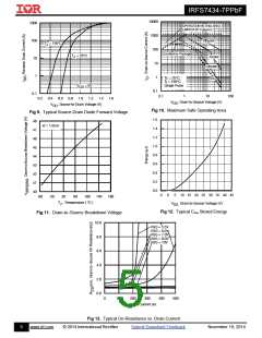
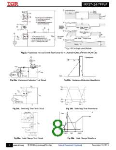
See Fig 15, 16, 23a, 23b
Repetitive Avalanche Energy
Thermal Resistance
Symbol
Parameter
Typ.
–––
–––
Max.
0.51
40
Units
°C/W
Junction-to-Case
Junction-to-Ambient
RJC
RJA
Static @ TJ = 25°C (unless otherwise specified)
Symbol
V(BR)DSS
Parameter
Drain-to-Source Breakdown Voltage
Breakdown Voltage Temp. Coefficient
Min. Typ. Max. Units
40 ––– –––
––– 0.03 ––– V/°C Reference to 25°C, ID = 1mA
Conditions
VGS = 0V, ID = 250µA
V
V(BR)DSS/TJ
–––
–––
2.2
0.7
1.5
3.0
1.0
–––
3.9
1.0
V
V
GS = 10V, ID = 100A
GS = 6V, ID = 50A
RDS(on)
Static Drain-to-Source On-Resistance
Gate Threshold Voltage
m
V
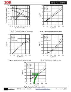
VGS(th)
VDS = VGS, ID = 250µA
DS =40 V, VGS = 0V
VDS =40V,VGS = 0V,TJ =125°C
––– –––
V
IDSS
Drain-to-Source Leakage Current
µA
––– ––– 150
––– ––– 100
––– ––– -100
Gate-to-Source Forward Leakage
Gate-to-Source Reverse Leakage
Gate Resistance
V
V
GS = 20V
GS = -20V
IGSS
nA
RG
–––
2.0
–––
Notes:
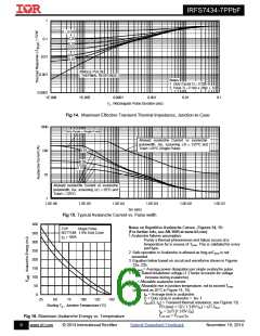
Calculated continuous current based on maximum allowable junction temperature. Bond wire current limit is 240A by
source bonding technology. Note that current limitations arising from heating of the device leads may occur with
some lead mounting arrangements. (Refer to AN-1140)
Repetitive rating; pulse width limited by max. junction temperature.
Limited by TJmax, starting TJ = 25°C, L = 0.077mH, RG = 50, IAS = 100A, VGS =10V.
ISD 100A, di/dt 969A/µs, VDD V(BR)DSS, TJ 150°C.
Pulse width 400µs; duty cycle 2%.
Coss eff. (TR) is a fixed capacitance that gives the same charging time as Coss while VDS is rising from 0 to 80% VDSS
.
Coss eff. (ER) is a fixed capacitance that gives the same energy as Coss while VDS is rising from 0 to 80% VDSS
.
R is measured at TJ approximately 90°C.
Limited by TJmax, starting TJ = 25°C, L = 1mH, RG = 50, IAS = 42A, VGS =10V.
When mounted on 1" square PCB (FR-4 or G-10 Material). Please refer to AN-994 for more details:
http://www.irf.com/technical-info/appnotes/an-994.pdf
*
Pulse drain current is limited by source bonding technology.
2
www.irf.com
© 2014 International Rectifier
Submit Datasheet Feedback
November 19, 2014

 INFINEON [ Infineon ]