IRFS7434-7PPbF
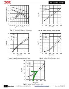
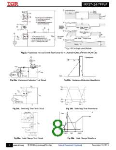
Fig 22. Peak Diode Recovery dv/dt Test Circuit for N-Channel HEXFET® Power MOSFETs
V
(BR)DSS
t
p
15V
DRIVER
+
L
V
DS
D.U.T
AS
R
G
V
DD
-
I
A
20V
I
0.01
t
p
AS
Fig 23a. Unclamped Inductive Test Circuit
Fig 23b. Unclamped Inductive Waveforms
Fig 24a. Switching Time Test Circuit
Fig 24b. Switching Time Waveforms
Id
Vds
Vgs
Vgs(th)
Qgs1
Qgs2
Qgd
Qgodr
Fig 25b. Gate Charge Waveform
Fig 25a. Gate Charge Test Circuit
8
www.irf.com
© 2014 International Rectifier
Submit Datasheet Feedback
November 19, 2014

 INFINEON [ Infineon ]