Quasi-Resonant PWM Controller
ICE2QS01
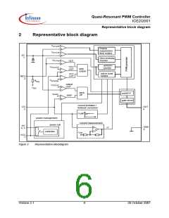
Functional Description
detected zero-crossing to the switch-on of the main 3.3.2
Switch-off Determination
switch tdelay, theoretically:
In the converter system, the primary current is sensed
by an external shunt resistor, which is connected
between low-side terminal of the main power switch
and the common ground. The sensed voltage across
the shunt resistor vCS is applied to an internal current
measurement unit, and its output voltage v1 is
compared with the regulation voltage vreg. Once the
voltage v1 exceeds the voltage vREG, the output flip-flop
is reset. As a result, the main power switch is switched
off. The relationship between the v1 and the vcs is
described by:
Tosc
4
∆t = --------- – tdelay
[3]
This time delay should be matched by adjusting the
time constant of the RC network which is calculated as:
R
zc1 ⋅ Rzc2
τtd = Czc ⋅ ---------------------------
[4]
Rzc1 + Rzc2
3.3.1.3
Switch-on Determination
v1 = 3.3 ⋅ vCS + 0.7
In the system, turn-on of the power switch depends on
the value of the up/down counter, the value of the zero-
crossing counter and the voltage at the ZC pin vZC.
Turn-on happens only when the value in the both
counters are the same and the voltage at the ZC is
lower than the threshold VZCT1. For comparison of the
values from both counters, a digital comparator is used.
Once these counters have the same value, the
[5]
To avoid mistriggering caused by the voltage spike
across the shunt resistor after switch-on of the main
power switch, a 330ns leading edge blanking time
applies to output of the comparator.
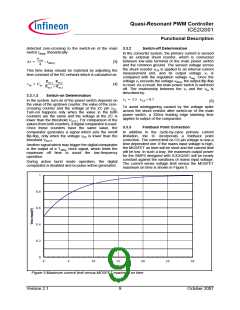
3.3.3
Foldback Point Correction
comparator generates a signal which sets the on/off In addition to the cycle-by-cylce primary current
flip-flop, only when the voltage vZC is lower than the limitation, the IC incorporats
foldback point
a
threshold VZCT1
.
correction. The current limit on CS pin voltage is now a
time dependent one. If the mains input voltage is high,
the MOSFET on time will be short and the current limit
will be low. In such a way, the maximum output power
for the SMPS designed with ICE2QS01 will be nearly
constant against the variations of mains input voltage.
The current sense voltage limit versus the MOSFET
maximum on time is shown in Figure 5.
Another signal which may trigger the digital comparator
is the output of a TsMax clock signal, which limits the
maximum off time to avoid the low-frequency
operation.
During active burst mode operation, the digital
comparator is disabled and no pulse will be generated.
1
0.8
0.6
0.4
0.2
0
0
5
10
15
20
25
30
Ton(us)
Figure 5 Maximum current limit versus MOSFET maximum on time
Version 2.1
9
October 2007

 INFINEON [ Infineon ]