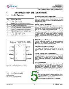
CCM-PFC
ICE2PCS01/G
Functional Description
connected) or an insufficient input voltage VIN for
normal operation. In this case, most of the blocks within
the IC will be shutdown. It is implemented using
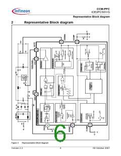
comparator C3 with a threshold of 0.6V as shown in the
IC block diagram in Figure 2.
POUT(rated)
POUT(max)
IC’s
Normal
State Operation
3.4.4
Over-Voltage Protection (OVP)
Whenever VOUT exceeds the rated value by 5%, the
over-voltage protection OVP is active as shown in
Figure 6. This is implemented by sensing the voltage at
pin VSENSE with respect to a reference voltage of
3.15V. A VSENSE voltage higher than 3.15V will
immediately reduce the output duty cycle, bypassing
the normal voltage loop control. This results in a lower
input power to reduce the output voltage VOUT. A
VSENSE voltage higher than 3.25V will immediately
turn off the gate, thereby preventing damage to bus
capacitor.
SOC
PCL
VISENSE
-0.61V -0.75V
-1.04V
0
Figure 8
SOC and PCL Protection as function of
VISENSE
The rated output power with a minimum VIN (VINMIN) is
0.61
P
OUT(rated) = VINMIN × ------------------
R1 ⋅
2
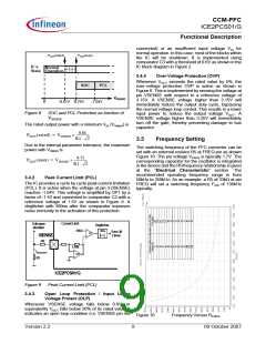
3.5
Frequency Setting
Due to the internal parameter tolerance, the maximum
power with VINMIN is
The switching frequency of the PFC converter can be
set with an external resistor R5 at FREQ pin as shown
Figure 10. The pin voltage VFREQ is typically 1.7V. The
corresponding capacitor for the oscillator is integrated
in the device and the R5/frequency relationship is given
at the “Electrical Characteristic” section. The
recommended operating frequency range is from
50kHz to 250kHz. As an example, a R5 of 33kΩ at pin
FREQ will set a switching frequency FSW of 136kHz
typically.
0.75
P
OUT(max) = VINMIN × ------------------
R1 ⋅
2
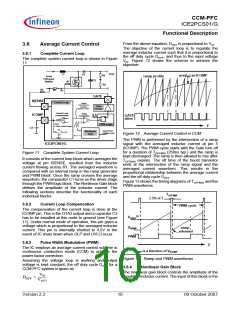
3.4.2
Peak Current Limit (PCL)
The IC provides a cycle by cycle peak current limitation
(PCL). It is active when the voltage at pin 3 (ISENSE)
reaches -1.04V. This voltage is amplified by OP1 by a
factor of -1.43 and connected to comparator C2 with a
reference voltage of 1.5V as shown in Figure 9. A
deglitcher with 300ns after the comparator improves
noise immunity to the activation of this protection.
Current Limit
1.5V
Full-wave
Rectifier
Deglitcher
300ns
Turn Off
Driver
C2
ISENSE
R2
1.43x
IINDUCTOR
R1
OP1
ICE2PCS01/G
Figure 9
Peak Current Limit (PCL)
3.4.3
Open Loop Protection / Input Under
Voltage Protect (OLP)
Whenever VSENSE voltage falls below 0.6V, or
equivalently VOUT falls below 20% of its rated value, it
indicates an open loop condition (i.e. VSENSE pin not
Figure 10
Frequency Versus RFREQ
Version 2.2
9
09 October 2007

 INFINEON [ Infineon ]