CCM-PFC
ICE2PCS01/G
Pin Configuration and Functionality
1
Pin Configuration and Functionality
1.1
Pin Configuration
ICOMP (Current Loop Compensation)
Low pass filter and compensation of the current control
loop. The capacitor which is connected at this pin
integrates the output current of OTA2 and averages the
current sense signal.
Pin
Symbol Function
1
2
3
4
5
6
7
8
GND
IC Ground
ICOMP Current Loop Compensation
ISENSE Current Sense Input
ISENSE (Current Sense Input)
The ISENSE Pin senses the voltage drop at the
external sense resistor (R1). This is the input signal for
the average current regulation in the current loop. It is
also fed to the peak current limitation block.
FREQ
Switching Frequency Setting
VCOMP Voltage Loop Compensation
VSENSE VOUT Sense (Feedback) Input
During power up time, high inrush currents cause high
negative voltage drop at R1, driving currents out of pin
3 which could be beyond the absolute maximum
ratings. Therefore a series resistor (R2) of around
220Ω is recommended in order to limit this current into
the IC.
VCC
IC Supply Voltage
Gate Drive Output
GATE
FREQ (Frequency Setting)
This pin allows the setting of the operating switching
frequency by connecting a resistor to ground. The
frequency range is from 50kHz to 250kHz.
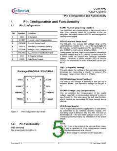
Package PG-DIP-8 / PG-DSO-8
VSENSE (Voltage Sense/Feedback)
The output bus voltage is sensed at this pin via a
resistive divider. The reference voltage for this pin is
3V.
GND
ICOMP
ISENSE
FREQ
1
8
7
6
5
GATE
VCC
2
VCOMP (Voltage Loop Compensation)
3
4
VSENSE
This pin provides the compensation of the output
voltage loop with a compensation network to ground
(see Figure 2). This also gives the soft start function
which controls an increasing AC input current during
start-up.
VCOMP
VCC (Power Supply)
The VCC pin is the positive supply of the IC and should
be connected to an external auxiliary supply. The
operating range is between 11V and 26V. The turn-on
threshold is at 11.8V and under voltage occurs at 11V.
There is no internal clamp for a limitation of the power
supply.
Figure 1
Pin Configuration (top view)
GATE
1.2
Pin Functionality
The GATE pin is the output of the internal driver stage,
which has a capability of 1.5A instantaneous source
and 2.0A instantaneous sink current.
GND (Ground)
The ground potential of the IC.
Its gate drive voltage is clamped at 15V (typically).
Version 2.2
5 09 October 2007

 INFINEON [ Infineon ]