BTS7012-2EPA
PROFET™ +2 12V
Logic Pins
5.2
Diagnosis Pin
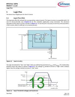
The Diagnosis Enable (DEN) pin controls the diagnosis circuitry and the protection circuitry. When DEN pin is
set to “high”, the diagnosis is enabled (see Chapter 9.2 for more details). When it is set to “low”, the diagnosis
is disabled (IS pin is set to high impedance).
The Diagnosis Selection (DSEL) pin selects the channel where diagnosis is performed (see Chapter 9.1.1).
The transition from “high” to “low” of DEN pin clears the protection latch of the channel selected with DSEL
pin depending on the logic state of IN pin and DEN pulse length (see Chapter 8.3 for more details). The internal
structure of diagnosis pins is the same as the one of input pins. See Figure 11 for more details.
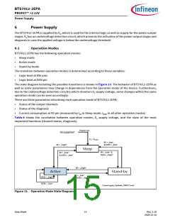
5.3
Electrical Characteristics Logic Pins
VS = 6 V to 18 V, TJ = -40 °C to +150 °C
Typical values: VS = 13.5 V, TJ = 25 °C
Digital Input (DI) pins = IN, DEN, DSEL
Table 7
Electrical Characteristics: Logic Pins - General
Parameter
Symbol
Values
Typ.
1.3
Unit Note or
Test Condition
Number
Min.
Max.
Digital Input Voltage
Threshold
VDI(TH)
0.8
2
V
See Figure 11 and P_5.4.0.1
Figure 12
1)
Digital Input Clamping
Voltage
VDI(CLAMP1)
–
7
–
V
P_5.4.0.2
IDI = 1 mA
See Figure 11 and
Figure 12
Digital Input Clamping
Voltage
VDI(CLAMP2)
VDI(HYS)
IDI(H)
6.5
–
7.5
0.25
10
8.5
–
V
IDI = 2 mA
See Figure 11 and
Figure 12
1)
P_5.4.0.3
P_5.4.0.4
P_5.4.0.5
P_5.4.0.6
Digital Input Hysteresis
V
See Figure 11 and
Figure 12
Digital Input Current
(“high”)
2
25
25
µA
µA
VDI = 2 V
See Figure 11 and
Figure 12
Digital Input Current (“low”) IDI(L)
2
10
VDI = 0.8 V
See Figure 11 and
Figure 12
1) Not subject to production test - specified by design.
Data Sheet
14
Rev. 1.10
2020-12-14

 INFINEON [ Infineon ]