BTS 640 S2
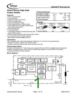
Pin
1
Symbol
ST
Function
Diagnostic feedback: open drain, invers to input level
2
GND
IN
Logic ground
3
Input, activates the power switch in case of logical high signal
Positive power supply voltage, the tab is shorted to this pin
4
V
bb
Sense current output, proportional to the load current, zero in
the case of current limitation of load current
5
IS
6 & 7
OUT
(Load, L)
Output, protected high-side power output to the load.
Both output pins have to be connected in parallel for operation
according this spec (e.g. kILIS).
Design the wiring for the max. short circuit current
Maximum Ratings at Tj = 25 °C unless otherwise specified
Parameter
Symbol
Values
Unit
V
Supply voltage (overvoltage protection see page 4)
Vbb
Vbb
43
34
Supply voltage for full short circuit protection
V
T
=-40 ...+150°C
j Start
3)
Load dump protection1)
V
= V + V , V = 13.5V
VLoad dump
60
V
LoadDump
A
s
A
2)
R
= 2 Ω, R = 1 Ω, t = 200 ms, IN= low or high
L d
I
Load current (Short circuit current, see page 5)
IL
self-limited
A
Operating temperature range
Storage temperature range
Tj
Tstg
-40 ...+150
-55 ...+150
°C
Power dissipation (DC), T ≤ 25 °C
Ptot
85
W
C
Inductive load switch-off energy dissipation, single pulse
V
= 12V, T = 150°C, T = 150°C const.
j,start C
bb
IL = 12.6 A, ZL = 4,2mH, 0 Ω: EAS
IL = 4 A, ZL = 330mH, 0 Ω: EAS
0,41
3,5
J
Electrostatic discharge capability (ESD)
IN: VESD
ST, IS:
1.0
4.0
8.0
kV
(Human Body Model)
out to all other pins shorted:
acc. MIL-STD883D, method 3015.7 and ESD assn. std. S5.1-1993
R=1.5kΩ; C=100pF
Input voltage (DC)
VIN
-10 ... +16
V
Current through input pin (DC)
Current through status pin (DC)
Current through current sense pin (DC)
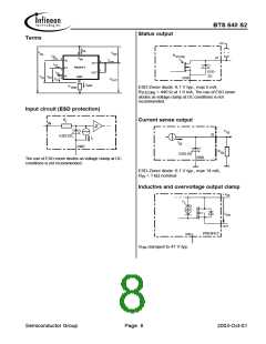
see internal circuit diagrams page 8
IIN
IST
IIS
±2.0
±5.0
±14
mA
1)
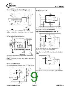
Supply voltages higher than Vbb(AZ) require an external current limit for the GND and status pins (a 150 Ω
resistor in the GND connection is recommended).
2)
3)
R = internal resistance of the load dump test pulse generator
I
VLoad dump is setup without the DUT connected to the generator according to ISO 7637-1 and DIN 40839
Semiconductor Group
Page 2
2003-Oct-01

 INFINEON [ Infineon ]