BTS 640 S2
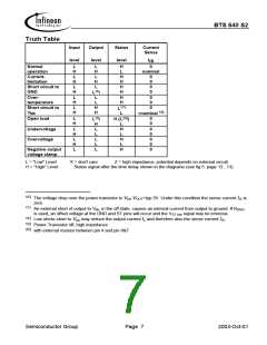
Truth Table
Input
level
Output
level
Status
level
Current
Sense
I
IS
Normal
L
H
L
H
L
L
H
L
H
L
H
L
H
H
H
H
0
operation
Current-
limitation
Short circuit to
GND
nominal
0
0
0
0
16
H
)
L
Over-
temperature
Short circuit to
L
H
L
L
L
H
H
H
H
0
0
0
17)
L
18)
V
bb
H
L
<nominal
19
20)
Open load
L
H
0
0
)
L
H (L
L
)
H
L
L
L
L
L
Undervoltage
Overvoltage
L
H
L
H
L
H
L
H
L
0
0
0
0
0
Negative output
voltage clamp
H
L = "Low" Level
H = "High" Level
X = don't care
Z = high impedance, potential depends on external circuit
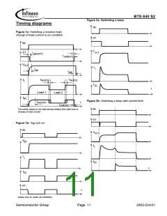
Status signal after the time delay shown in the diagrams (see fig 5. page 12...13)
16)
The voltage drop over the power transistor is Vbb-VOUT>typ.3V. Under this condition the sense current IIS is
zero
17)
An external short of output to Vbb, in the off state, causes an internal current from output to ground. If RGND
is used, an offset voltage at the GND and ST pins will occur and the VST low signal may be errorious.
18)
19)
20)
Low ohmic short to Vbb may reduce the output current IL and therefore also the sense current IIS.
Power Transistor off, high impedance
with external resistor between pin 4 and pin 6&7
Semiconductor Group
Page 7
2003-Oct-01

 INFINEON [ Infineon ]