BTS 5210G
Thermal Characteristics
Parameter and Conditions
Symbol
Values
Unit
min
typ
max
Thermal resistance
junction - soldering point6)7)
junction – ambient6)
each channel: Rthjs
Rthja
one channel active:
all channels active:
K/W
--
--
--
--
--
--
45
40
15
--
--
@ 6 cm2 cooling area
--
Electrical Characteristics
Parameter and Conditions, each of the four channels Symbol
Values
Unit
at Tj = -40...+150°C, V = 12 V unless otherwise specified
bb
min
typ
max
Load Switching Capabilities and Characteristics
On-state resistance (V to OUT); I = 2 A
L
bb
each channel,
--
--
--
mΩ
Tj = 25°C: RON
Tj = 150°C:
two parallel channels, Tj = 25°C:
110
210
55
140
280
70
see diagram, page 11
Nominal load current
one channel active: IL(NOM)
two parallel channels active:
1.8
3.4
2.4
3.9
--
A
6)
Device on PCB , T = 85°C, T ≤ 150°C
a
j
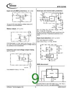
Output current while GND disconnected or pulled up8);
IL(GNDhigh)
--
--
2
mA
V
= 32 V, V = 0,
IN
bb
see diagram page 9
Turn-on time9)
Turn-off time
RL = 12 Ω
IN
IN
to 90% VOUT: ton
to 10% VOUT: toff
--
--
100
100
250
270
µs
Slew rate on9)
Slew rate off9)
10 to 30% VOUT, RL = 12 Ω: dV/dton
70 to 40% VOUT, RL = 12 Ω: -dV/dtoff
0.2
0.2
--
--
1.0 V/µs
1.1 V/µs
Device on 50mm*50mm*1.5mm epoxy PCB FR4 with 6cm2 (one layer, 70µm thick) copper area for V
connection. PCB is vertical without blown air. See page 14
Soldering point: upper side of solder edge of device pin 15. See page 14
not subject to production test, specified by design
6)
bb
7)
8)
9)
See timing diagram on page 12.
Infineon Technologies AG
5
2003-Oct-01

 INFINEON [ Infineon ]