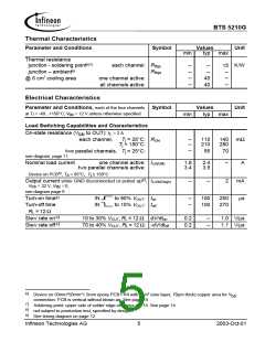
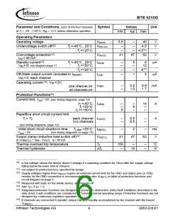
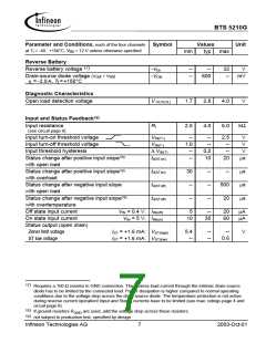
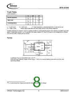
BTS 5210G
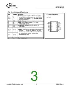
Pin Definitions and Functions
Pin configuration
Pin
Symbol Function
Positive power supply voltage. Design the
1,7,
8,14
wiring for the simultaneous max. short circuit
currents from channel 1 to 2 and also for low
thermal resistance
(top view)
V
bb
2
3
5
4
6
GND
IN1
IN2
ST1
ST2
Logic Ground
Input 1,2 activates channel 1,2 in case
of logic high signal
V
GND
IN1
ST1
IN2
ST2
1 • 14 V
bb
bb
2
3
4
5
6
7
13 OUT1
12 OUT1
11 NC
Diagnostic feedback 1,2 of channel 1,2
open drain
10 OUT2
9 OUT2
Output 1,2 protected high-side power output of
channel 1,2. Design the wiring for the max.
short circuit current; both output pins have to
be connected in parallel for operation
according this spec.
12,13 OUT1
V
8 V
bb
bb
9,10
11
OUT2
NC
Not Connected
Infineon Technologies AG
3
2003-Oct-01

 INFINEON [ Infineon ]