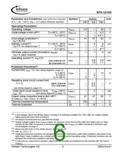
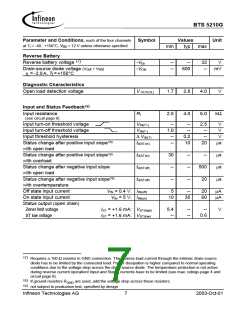
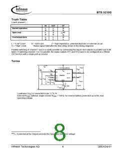
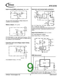
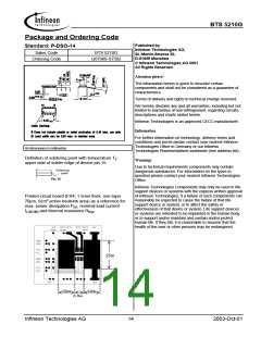
BTS 5210G
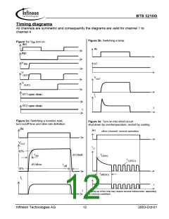
Timing diagrams
All channels are symmetric and consequently the diagrams are valid for channel 1 to
channel 4
Figure 2b: Switching a lamp:
Figure 1a: V turn on:
bb
IN1
IN
IN2
V
ST
V
bb
V
OUT1
OUT
V
OUT2
ST1 open drain
ST2 open drain
I
L
t
t
Figure 2a: Switching a resistive load,
turn-on/off time and slew rate definition:
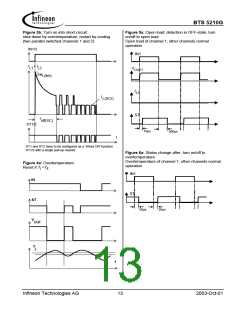
Figure 3a: Turn on into short circuit:
shut down by overtemperature, restart by cooling
IN
IN1
other channel: normal operation
VOUT
I
L1
90%
I
t
dV/dtoff
on
L(lim)
I
L(SCr)
t
dV/dton
off
10%
t
off(SC)
ST
IL
t
t
Heating up of the chip may require several milliseconds, depending
on external conditions
Infineon Technologies AG
12
2003-Oct-01

 INFINEON [ Infineon ]