BTS 432 E2
Parameter and Conditions
Symbol
Values
Unit
at Tj = 25 °C, V = 12 V unless otherwise specified
bb
min
typ
max
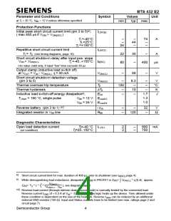
Protection Functions
Initial peak short circuit current limit (pin 3 to 5)8),
IL(SCp)
( max 400 µs if VON > VON(SC)
)
Tj =-40°C:
Tj =25°C:
Tj =+150°C:
--
--
24
--
44
--
74
--
--
A
Repetitive short circuit current limit
IL(SCr)
Tj = Tjt (see timing diagrams, page 10)
22
80
35
--
--
A
Short circuit shutdown delay after input pos. slope
VON > VON(SC) Tj =-40..+150°C: td(SC)
,
400
µs
min value valid only, if input "low" time exceeds 30 µs
Output clamp (inductive load switch off)
at VOUT = Vbb - VON(CL), IL= 30 mA
VON(CL)
--
58
--
V
Short circuit shutdown detection voltage
(pin 3 to 5)
VON(SC)
Tjt
--
150
--
8.3
--
--
--
V
°C
K
Thermal overload trip temperature
Thermal hysteresis
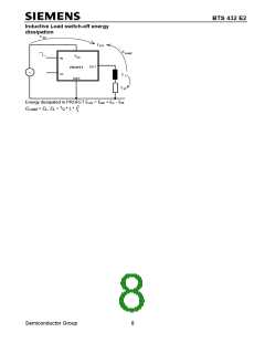
Inductive load switch-off energy dissipation9),
∆Tjt
10
--
--
EAS
--
1.7
1.3
1.0
J
Tj Start = 150 °C, single pulse
Vbb = 12 V: ELoad12
Vbb = 24 V: ELoad24
Reverse battery (pin 3 to 1) 10)
Integrated resistor in Vbb line
-Vbb
Rbb
--
--
--
32
--
V
120
Ω
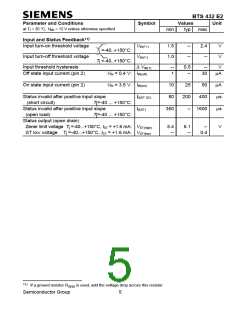
Diagnostic Characteristics
Open load detection current
Tj=-40 °C: IL (OL)
Tj=25..150°C:
2
2
--
--
900 mA
750
(on-condition)
8)
Short circuit current limit for max. duration of 400 µs, prior to shutdown (see t
page 4)
d(SC)
9)
While demagnetizing load inductance, dissipated energy in PROFET is E = VON(CL) * iL(t) dt, approx.
AS
∫
VON(CL)
VON(CL) - Vbb
2
L
1
E
AS
= / * L * I * (
), see diagram page 8
2
10)
Reverse load current (through intrinsic drain-source diode) is normally limited by the connected load.
Reverse current I of ≈ 0.3 A at V = -32 V through the logic heats up the device. Time allowed under
GND
bb
these condition is dependent on the size of the heatsink. Reverse I
can be reduced by an additional
GND
external GND-resistor (150 Ω). Input and Status currents have to be limited (see max. ratings page 2 and
circuit page 7).
Semiconductor Group
4

 INFINEON [ Infineon ]