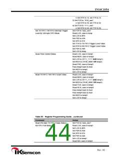
IN16C1054
LCR
MCR
LSR
MSR
[7:0] = ‘0000_0000’
[7:0] = ‘0000_0000’
[7:0] = ‘0110_0000’
[7:4] = ‘0000’
[3:0] = Logic levels of the inputs inverted
[7:0] = ‘0000_0000’
Page 1
SPR
DLL
[7:0] = ‘1111_1111’
[7:0] = ‘1111_1111’
Page 2
DLM
GICR
GISR
TCR
RCR
FSR
[7:0] = ‘0000_0000’
[7:0] = ‘0000_0000’
[7:0] = ‘0000_0000’
[7:0] = ‘0000_0000’
[7:0] = ‘0000_0000’
Page 3
PSR
[7:0] = ‘0000_0000’
[7:0] = ‘0000_0000’
[7:0] = ‘0000_0000’
[7:0] = ‘0000_0000’
[7:0] = ‘0000_0000’
[7:0] = ‘0000_0000’
[7:0] = ‘0000_0000’
Page 4
ATR
EFR
XON1
XON2
XOFF1
XOFF2
AFR
[7:0] = ‘0000_0000’
[7:0] = ‘0000_0000’
[7:0] = ‘1000_0000’
[7:0] = ‘1000_0000’
[7:0] = ‘0000_0000’
[7:0] = ‘0000_0000’
Reset State
XRCR
TTR
RTR
FUR
FLR
Output Signals
TXD, RTS#, DTR#
TXRDY#
RXRDY#
INT
Logic 1
Logic 0
Logic 1
Tri-State Condition = INTSEL is open or low state
Logic 0 = INTSEL is high state
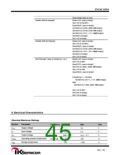
8. Programmer’s Guide
The base set of registers that is used during high-speed data transfer has a
straightforward access method. The extended function registers require special access
bits to be decoded along with the address lines. The following guide will help with
programming these registers. Note that the descriptions below are for individual register
access. Some streamlining through interleaving can be obtained when programming all
the registers.
Rev. 00

 IKSEMICON [ IK SEMICON CO., LTD ]