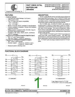
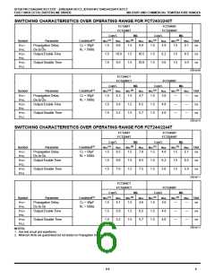
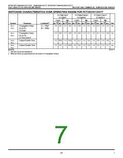
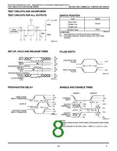
IDT54/74FCT240/244T/AT/CT/DT - 2240/2244T/AT/CT, IDT54/74FCT540/541/2541T/AT/CT
FAST CMOS OCTAL BUFFER/LINE DRIVER
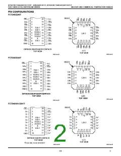
MILITARY AND COMMERCIAL TEMPERATURE RANGES
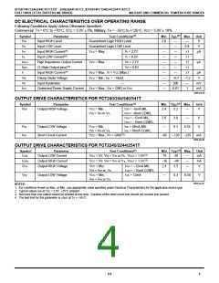
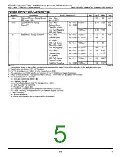
POWER SUPPLY CHARACTERISTICS
Symbol
Parameter
Quiescent Power Supply Current
TTL Inputs HIGH
Test Conditions(1)
Min. Typ.(2) Max.
Unit
∆ICC
VCC = Max.
VIN = 3.4V(3)
—
0.5
2.0
mA
ICCD
Dynamic Power Supply
Current(4)
VCC = Max.
VIN = VCC FCTxxxT
VIN = GND
—
0.15
0.25
mA/
MHz
Outputs Open
OEA = OEB = GND
One Input Toggling
50% Duty Cycle
VCC = Max.
FCT2xxxT
—
0.06
0.12
IC
Total Power Supply Current(6)
VIN = VCC FCTxxxT
VIN = GND FCT2xxxT
—
—
1.5
0.6
3.5
2.2
mA
Outputs Open
fi = 10MHz
50% Duty Cycle
OEA = OEB = GND
One Bit Toggling
VIN = 3.4
FCTxxxT
—
1.8
4.5
VIN = GND FCT2xxxT
VIN = VCC FCTxxxT
VIN = GND FCT2xxxT
0.9
3.0
1.2
3.2
VCC = Max.
—
—
6.0(5)
3.4(5)
Outputs Open
fi = 2.5MHz
50% Duty Cycle
OEA = OEB = GND
Eight Bits Toggling
VIN = 3.4
FCTxxxT
—
—
5.0
3.2
14.0(5)
11.4(5)
VIN = GND FCT2xxxT
2565 tbl 08
NOTES:
1. For conditions shown as Max. or Min., use appropriate value specified under Electrical Characteristics for the applicable device type.
2. Typical values are at VCC = 5.0V, +25°C ambient.
3. Per TTL driven input (VIN = 3.4V). All other inputs at VCC or GND.
4. This parameter is not directly testable, but is derived for use in Total Power Supply Calculations.
5. Values for these conditions are examples of the ICC formula. These limits are guaranteed but not tested.
6. IC = IQUIESCENT + IINPUTS + IDYNAMIC
IC = ICC + ∆ICC DHNT + ICCD (fCP/2 + fiNi)
ICC = Quiescent Current
∆ICC = Power Supply Current for a TTL High Input (VIN = 3.4V)
DH = Duty Cycle for TTL Inputs High
NT = Number of TTL Inputs at DH
ICCD = Dynamic Current Caused by an Input Transition Pair (HLH or LHL)
fCP = Clock Frequency for Register Devices (Zero for Non-Register Devices)
fi = Input Frequency
Ni = Number of Inputs at fi
All currents are in milliamps and all frequencies are in megahertz.
6.8
5

 IDT [ INTEGRATED DEVICE TECHNOLOGY ]