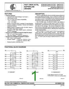
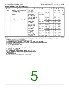
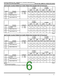
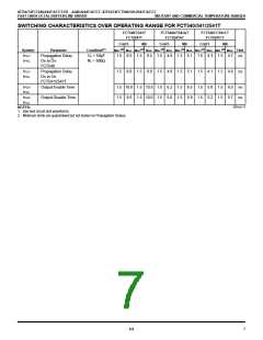
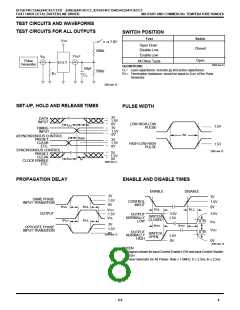
IDT54/74FCT240/244T/AT/CT/DT - 2240/2244T/AT/CT, IDT54/74FCT540/541/2541T/AT/CT
FAST CMOS OCTAL BUFFER/LINE DRIVER
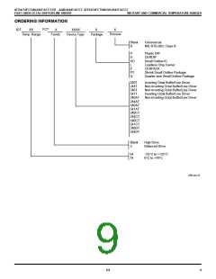
MILITARY AND COMMERCIAL TEMPERATURE RANGES
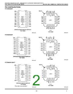
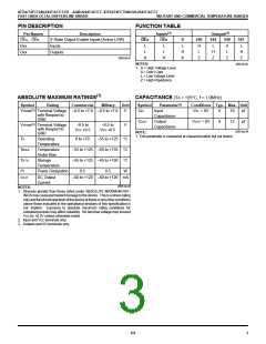
PIN DESCRIPTION
FUNCTION TABLE
Pin Names
Description
Inputs(1)
Outputs(1)
OEA, OEB
Dxx
3–State Output Enable Inputs (Active LOW)
A
B
OE
D
L
240
H
244
L
540
H
541
OE
Inputs
L
L
L
L
L
H
H
X
L
H
L
H
Z
Oxx
Outputs
2565 tbl 01
H
Z
Z
Z
NOTES:
2565 tbl 02
1. H = High Voltage Level
X = Don’t Care
L = Low Voltage Level
Z = High Impedance
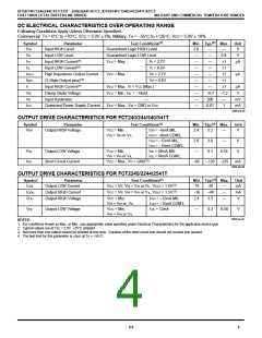
ABSOLUTE MAXIMUM RATINGS(1)
CAPACITANCE (TA = +25°C, f = 1.0MHz)
Symbol
Rating
Commercial
Military
Unit
Symbol
Parameter(1)
Input
Capacitance
Output
Conditions Typ. Max. Unit
(2)
VTERM
Terminal Voltage
with Respect to
GND
–0.5 to +7.0 –0.5 to +7.0
V
CIN
VIN = 0V
6
10
pF
COUT
VOUT = 0V
8
12
pF
(3)
VTERM
Terminal Voltage
with Respect to
GND
–0.5 to
VCC +0.5
–0.5 to
VCC +0.5
V
Capacitance
2565 lnk 04
NOTE:
1. This parameter is measured at characterization but not tested.
TA
Operating
0 to +70
–55 to +125 °C
Temperature
Temperature
Under Bias
Storage
TBIAS
TSTG
–55 to +125 –65 to +135 °C
–55 to +125 –65 to +150 °C
Temperature
Power Dissipation
PT
0.5
0.5
W
IOUT
DC Output
Current
–60 to +120 –60 to +120 mA
2565 lnk 03
NOTES:
1. Stresses greater than those listed under ABSOLUTE MAXIMUM RAT-
INGS may cause permanent damage to the device. This is a stress rating
onlyandfunctionaloperationofthedeviceattheseoranyotherconditions
above those indicated in the operational sections of this specification is
not implied. Exposure to absolute maximum rating conditions for
extended periods may affect reliability. No terminal voltage may exceed
VCC by +0.5V unless otherwise noted.
2. Input and VCC terminals only.
3. Outputs and I/O terminals only.
6.8
3

 IDT [ INTEGRATED DEVICE TECHNOLOGY ]