IDT7203/7204/7205/7206/7207/7208CMOSASYNCHRONOUSFIFO
2,048 x 9, 4,096 x 9, 8,192 x 9, 16,384 x 9, 32,768 x 9, 65,536 x 9
COMMERCIAL,INDUSTRIALANDMILITARY
TEMPERATURERANGES
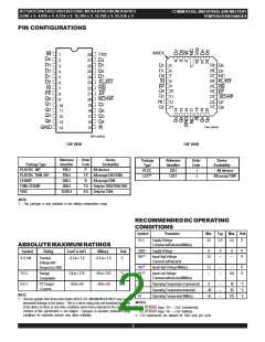
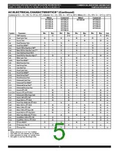
PIN CONFIGURATIONS
INDEX
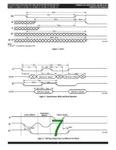
W
Vcc
1
28
27
26
25
24
23
22
21
20
19
18
17
16
15
D8
D
4
2
3
4
5
D
3
29
D
5
D
2
D6
5
6
7
28
27
26
25
24
23
D
2
D1
D
6
D7
D
0
NC
D
1
D
7
8
9
10
11
XI
FL/RT
RS
EF
D
0
FL/RT
RS
EF
XO/HF
6
7
FF
XI
Q
0
FF
8
9
Q
1
XO/HF
Q
0
NC 12
Q2
22
21
Q7
Q
1
Q7
10
11
12
13
14
13
Q
6
Q
2
Q
6
Q
3
Q
5
Q8
Q
4
2661 drw02b
GND
R
2661 drw02a
TOP VIEW
TOP VIEW
Reference
Identifier
Order
Code
Device
Availability
All devices
Package
Type
Reference
Identifier
Order
Code
Device
Availability
PackageType
PLASTIC DIP
P28-1
P28-2
D28-1
D28-3
SO28-3
P
PLCC
J32-1
L32-1
J
All devices
(1)
PLASTIC THIN DIP
CERDIP
TP Allexcept7207/7208
Allexcept7208
LCC
L
All except 7208
D
THIN CERDIP
SOIC
TD Onlyfor7203/7204/7205
SO Only for 7204
NOTE:
1. This package is only available in the military temperature range.
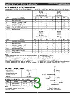
RECOMMENDEDDCOPERATING
CONDITIONS
Symbol
Parameter
Min. Typ. Max. Unit
VCC
SupplyVoltage
4.5
5.0
5.5
V
Commercial/Industrial/Military
SupplyVoltage
ABSOLUTEMAXIMUMRATINGS
GND
0
0
0
V
V
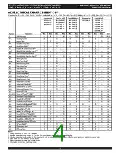
Symbol
Rating
Com'l & Ind'l
Military
Unit
(1)
VIH
InputHighVoltage
Commercial/Industrial
2.0
—
—
VTERM
Terminal
–0.5to+7.0
–0.5to+7.0
V
Voltagewith
Respect to GND
(1)
VIH
InputHighVoltageMilitary
2.2
—
—
—
—
V
V
(2)
TSTG
IOUT
Storage
Temperature
–55to+125
–50to+50
–65to+155
–50to+50
°C
VIL
InputLowVoltage
Commercial/Industrial/Military
0.8
DCOutput
+Current
mA
TA
TA
TA
OperatingTemperatureCommercial
OperatingTemperatureIndustrial
OperatingTemperatureMilitary
0
—
—
—
70
85
°C
°C
–40
–55
NOTE:
125 °C
1. Stresses greater than those listed under ABSOLUTE MAXIMUM RATINGS may cause
permanent damage to the device. This is a stress rating only and functional operation
of the device at these or any other conditions above those indicated in the operational
sections of this specification is not implied. Exposure to absolute maximum rating
conditions for extended periods may affect reliability.
NOTES:
1. For RT/RS/XI input, VIH = 2.6V (commercial).
For RT/RS/XI input, VIH = 2.6V (military).
2. 1.5V undershoots are allowed for 10ns once per cycle.
2

 IDT [ INTEGRATED DEVICE TECHNOLOGY ]