932SQ420D
PCIE GEN 2/3 & QPI CLOCK FOR ROMLEY-BASED SERVERS
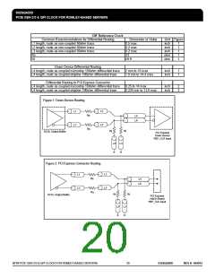
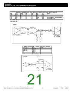
Alternative Termination for LVDS and other Common Differential Signals (figure 3)
Vdiff
0.45v
0.58
0.80
0.60
Vp-p
0.22v
0.28
0.40
0.3
Vcm
1.08
0.6
0.6
1.2
R1
33
33
33
33
R2
R3
R4
Note
150
78.7
78.7
174
100
137
none
140
100
100
100
100
ICS874003i-02 input compatible
Standard LVDS
R1a = R1b = R1
R2a = R2b = R2
Figure 3
L2
L1
R3
R4
R1a
R1b
L4
L4'
L2'
L1'
R2a
R2b
HCSL Output Buffer
Down Device
REF_CLK Input
L3'
L3
Cable Connected AC Coupled Application (figure 4)
Component
R5a, R5b
R6a, R6b
Cc
Value
8.2K 5%
1K 5%
Note
0.1 µF
Vcm
0.350 volts
Figure 4
3.3 Volts
R5a
R5b
R6b
Cc
Cc
L4
L4'
R6a
PCIe Device
REF_CLK Input
IDT® PCIE GEN 2/3 & QPI CLOCK FOR ROMLEY-BASED SERVERS
21
932SQ420D
REV H 042012

 IDT [ INTEGRATED DEVICE TECHNOLOGY ]