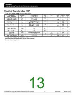
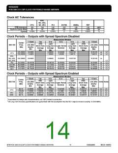
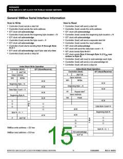
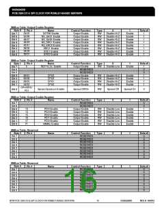
932SQ420D
PCIE GEN 2/3 & QPI CLOCK FOR ROMLEY-BASED SERVERS
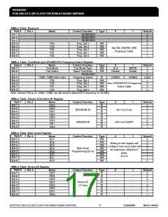
SMBus Table: Reserved
Byte 5
Bit 7
Pin #
Name
Control Function
RESERVED
RESERVED
RESERVED
Freq. Sel 4
Type
0
1
Default
0
0
0
0
1
1
1
1
Bit 6
Bit 5
Bit 4
Bit 3
Bit 2
Bit 1
Bit 0
-
FS4
FS3
FS2
FS1
FS0
RW
RW
RW
RW
RW
-
-
-
-
Freq. Sel 3
Freq. Sel 2
Freq. Sel 1
Freq. Sel 0
See NS_SAS/NS_SRC
Frequency Table.
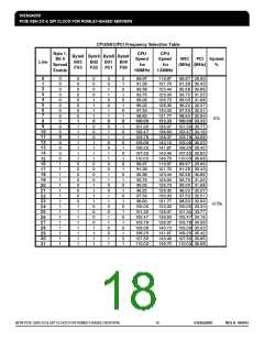
SMBus Table: Test Mode and CPU/SRC/PCI Frequency Select Register
Byte 6
Bit 7
Pin #
-
Name
Test Mode
Test Select
Control Function
Test Mode Type
Select Test Mode
RESERVED
Frequency Select
Freq. Sel 3
Type
RW
RW
0
Hi-Z
Disable
1
Default
REF/N
Enable
0
0
0
-
-
-
-
-
-
-
Bit 6
Bit 5
Bit 4
Bit 3
Bit 2
Bit 1
Bit 0
100M_133M# (See note)
133MHz
100MHz
Latch
R
FS3
FS2
FS1
FS0
RW
RW
RW
RW
1
0
0
0
See CPU/SRC/PCI Frequency
Select Table
Freq. Sel 2
Freq. Sel 1
Freq. Sel 0
Note: Internal Pull up on 100M_133M# pin will result in default CPU frequency of 100 MHz.
SMBus Table: Vendor & Revision ID Register
Byte 7
Bit 7
Pin #
-
Name
Control Function
Type
R
R
R
R
R
R
R
R
0
1
Default
RID3
RID2
RID1
RID0
VID3
VID2
VID1
0
0
1
1
0
0
0
-
-
-
-
-
-
-
Bit 6
Bit 5
Bit 4
Bit 3
Bit 2
Bit 1
Bit 0
REVISION ID
0011 for D rev
VENDOR ID
0001 for ICS/IDT
VID0
1
SMBus Table: Byte Count Register
Byte 8
Bit 7
Pin #
-
Name
BC7
BC6
BC5
BC4
BC3
BC2
BC1
BC0
Control Function
Type
RW
RW
RW
RW
RW
RW
RW
RW
0
1
Default
0
0
0
0
1
0
1
0
-
-
-
-
-
-
-
Bit 6
Bit 5
Bit 4
Bit 3
Bit 2
Bit 1
Bit 0
Writing to this register will
configure how many bytes will
be read back, default is A
bytes.
Byte Count
Programming b(7:0)
(0 to 9
SMBus Table: Device ID Register
Byte 9
Bit 7
Bit 6
Bit 5
Bit 4
Bit 3
Bit 2
Bit 1
Bit 0
Pin #
Name
DID7
DID6
DID5
DID4
DID3
DID2
DID1
DID0
Control Function
Type
R
R
R
R
R
R
R
R
0
-
-
-
-
-
-
-
-
1
-
-
-
-
-
-
-
-
Default
0
0
0
1
0
1
1
1
Device ID
(17 hex)
IDT® PCIE GEN 2/3 & QPI CLOCK FOR ROMLEY-BASED SERVERS
17
932SQ420D
REV H 042012

 IDT [ INTEGRATED DEVICE TECHNOLOGY ]