PRELIMINARY INFORMATION
ICS3726-12
HIGH PERFORMANCE VCXO
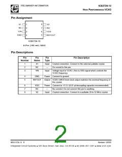
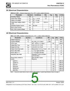
Pin Assignment
8
7
6
5
X1
NC
1
2
3
4
X2
NC
VI N
GND
VDD
REFOUT
I CS3726- 12
8-Pi n ( 150 mi l ) SOI C
Pin Descriptions
Pin
Pin
Pin
Pin Description
Number
Name
Type
Input
—
1
2
3
X1
NC
VIN
Crystal connection. Connect to the external pullable crystal.
Do connet to this pin.
Input
Voltage input to VCXO. Zero to VDD signal which controls the
VCXO frequency.
4
5
GND
Power Connect to ground.
REFOUT
Output VCXO CMOS level clock output matches the nominal frequency of
the crystal.
6
7
8
VDD
NC
Power Connect to +3.3 V (0.01 µf decoupling capacitor recommended).
—
No connect. Do not connect this pin to anything.
X2
Input
Crystal connection. Connect to a pullable 20 to 52 MHz crystal.
MDS 3726-12 B
2
Revision 120505
Integrated Circuit Systems ● 525 Race Street, San Jose, CA 95126 ● tel (408) 297-1201 ● www.icst.com

 IDT [ INTEGRATED DEVICE TECHNOLOGY ]