ICS341
FIELD PROGRAMMABLE SS VERSACLOCK SYNTHESIZER
EPROM CLOCK SYNTHESIZER
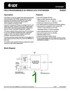
Pin Assignment
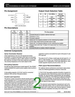
Output Clock Selection Table
S1
S0
CLK (MHz)
Spread
Percentage
User
Configurable
User
X1/ I CLK
VDD
8
7
6
5
1
2
3
4
X2
0
0
User
Configurable
User
Configurable
User
PDTS
S1
GND
S0
0
1
Configurable
User
CLK
1
0
Configurable
User
Configurable
Configurable
User
Configurable
1
1
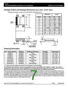
8-pin (150 mil) SOIC
Pin Descriptions
Pin
Number
Pin
Name
Pin
Type
Pin Description
1
2
3
4
5
6
X1/ICLK
VDD
GND
S0
XI
Connect this pin to a crystal or external clock input.
Connect to +3.3 V.
Power
Power
Input
Connect to ground.
Select pin 0 for frequency selection on CLK. Internal pull-up resistor.
CLK
S1
Output Clock output. Weak internal pull-down when tri-state.
Input
Input
XO
Select pin 1 for frequency selection on CLK. Internal pull-up resistor.
Powers down entire chip. Tri-states CLK outputs when low. Internal pull-up
resistor.
7
8
PDTS
X2
Connect this pin to a crystal, or float for clock input.
External Components
capacitors must be connected from each of the pins X1 and
X2 to ground.
Series Termination Resistor
Clock output traces over one inch should use series
termination. To series terminate a 50 trace (a commonly
used trace impedance), place a 33 resistor in series with
the clock line, as close to the clock output pin as possible.
The nominal impedance of the clock output is 20.
The value (in pF) of these crystal caps should equal (C -6
L
pF)*2. In this equation, C = crystal load capacitance in pF.
L
Example: For a crystal with a 16 pF load capacitance, each
crystal capacitor would be 20 pF [(16-6) x 2] = 20.
Decoupling Capacitor
PCB Layout Recommendations
As with any high-performance mixed-signal IC, the ICS341
must be isolated from system power supply noise to perform
optimally.
For optimum device performance and lowest output phase
noise, the following guidelines should be observed.
A decoupling capacitor of 0.01µF must be connected
between VDD and the PCB ground plane.
1) The 0.01µF decoupling capacitor should be mounted on
the component side of the board as close to the VDD pin as
possible. No vias should be used between the decoupling
capacitor and VDD pin. The PCB trace to VDD pin should be
kept as short as possible, as should the PCB trace to the
ground via. Distance of the ferrite bead and bulk decoupling
from the device is less critical.
Crystal Load Capacitors
The device crystal connections should include pads for
small capacitors from X1 to ground and from X2 to ground.
These capacitors are used to adjust the stray capacitance of
the board to match the nominally required crystal load
capacitance. Because load capacitance can only be
increased in this trimming process, it is important to keep
stray capacitance to a minimum by using very short PCB
traces (and no vias) between the crystal and device. Crystal
2) The external crystal should be mounted just next to the
device with short traces. The X1 and X2 traces should not
be routed next to each other with minimum spaces, instead
they should be separated and away from other traces.
IDT® / ICS™ FIELD PROGRAMMABLE SS VERSACLOCK SYNTHESIZER
2
ICS341
REV M 090613

 IDT [ INTEGRATED DEVICE TECHNOLOGY ]