IC80C51
IC80C31
loads TB8 into the ninth bit position of the transmit shift
register and flags the TX Control unit that a transmission is
requested. Transmission commences at S1P1 of the
machine cycle following the next rollover in the divide-by-
16 counter. Thus, the bit times are synchronized to the
divide-by-16 counter, not to the "write to SBUF" signal.
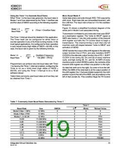
Table 8. Serial Port Setup
Mode
SCON
SM2Variation
0
1
2
3
0
1
2
3
10H
50H
90H
D0H
NA
Single Processor
Environment
(SM2 = 0)
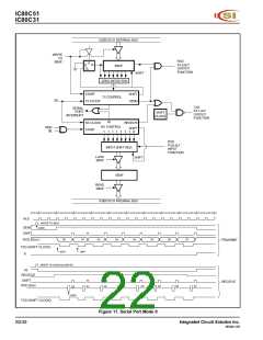
The transmission begins when SEND is activated, which
puts the start bit at TXD. One bit timer later, DATA is
activated, which enables the output bit of the transmit shift
register to TXD. The first shift pulse occurs one bit time after
that. The first shift clocks a 1 (the stop bit) into the ninth bit
position of the shift register. Thereafter, only 0s are clocked
in. Thus, as data bits shift out to the right, 0s are clocked in
from the left. When TB8 is at the output position of the shift
register, then the stop bit is just to the left of TB8, and all
positions to the left of that contain 0s. This condition flags
the TX Control unit to do one last shift, then deactivate
SEND and set TI. This occurs at the eleventh divide-by-16
rollover after "write to SBUF".
Multiprocessor
Environment
(SM2 = 1)
70H
B0H
F0H
Reception is initiated by a 1-to-0 transition detected at
RXD. For this purpose, RXD is sampled at a rate of 16 times
the established baud rate. When a transition is detected,
the divide-by-16 counter is immediately reset, and 1FFH is
written to the input shift register.
At the seventh, eighth, and ninth counter states of each bit
time, the bit detector samples the value of RXD. The value
accepted is the value that was seen in at least two of the
three samples. If the value accepted during the first bit time
is not 0, the receive circuits are reset and the unit continues
looking for another 1-to-0 transition. If the start bit proves
valid, it is shifted into the input shift register, and reception
of the rest of the frame proceeds.
As data bits come in from the right, 1s shift out to the left.
When the start bit arrives at the leftmost position in the shift
register (which in Modes 2 and 3 is a 9-bit register), it flags
the RX Control block to do one last shift, load SBUF and
RB8, and set RI. The signal to load SBUF and RB8 and to
set RI is generated if, and only if, the following conditions
are met at the time the final shift pulse is generated:
1) RI = 0, and
2) Either SM2 = 0 or the received ninth data bit = 1
If either of these conditions is not met, the received frame
is irretrievably lost, and RI is not set. If both conditions are
met, the received ninth data bit goes into RB8, and the first
eight data bits go into SBUF. One bit time later, whether the
above conditions were met or not, the unit continues
looking for a 1-to-0 transition at the RXD input.
Note that the value of the received stop bit is irrelevant to
SBUF, RB8, or RI.
Integrated Circuit Solution Inc.
MC001-0B
21

 ICSI [ INTEGRATED CIRCUIT SOLUTION INC ]