ICS1531 Data Sheet - Preliminary
Chapter 2 Summary
2.3.4 Voltage-Controlled Oscillator (Matches Input Signals to PFD)
The voltage level resulting from the output signals from the combined processing by the PFD, charge
pump, and loop filter drives the voltage-controlled oscillator (VCO). The VCO uses the level of this input
voltage to proportionally adjust its frequency output. This signal is compared to the input to the PFD so that
both inputs to the PFD match in both phase and frequency. The VCO can operate up to nearly 600 MHz
with a fixed gain. Consequently, the ICS1531 can be optimized for the best performance at all operating
frequencies. (For more information on the VCO, see Chapter 11, “VCO Transfer Characteristics”.)
2.3.5 Post-Scaler Divider (Sets Ratio of VCO and Pixel Clock Frequencies)
Using the frequency output from the VCO, the programmable Post-Scaler Divider (PSD) can set the ratio of
VCO frequency-to-pixel clock frequency at 2:1, 4:1, 8:1, or 16:1 (Reg 01:5-4). The maximum pixel clock
output frequency is therefore 300 MHz. However, for practical applications, the analog-to-digital converter
limits this output frequency to either 100, 140, or 165 MHz.
2.3.6 Feedback Divider (Controls Number of Pixel Clocks per HSYNC)
The ICS1531’s internal 12-bit pixel Feedback Divider (Regs 02 and 03) controls the total number of pixel
clocks per line (that is, between successive HSYNCs). The total number of pixels per line includes both
displayed and non-displayed pixels.
Reg 06:2 can delay the recovered HYSNC signal (that is, ADCSYNC) by one input clock period. This delay
has the effect of moving channel ‘A’ data to the ‘B’ channel output pins and the channel ‘B’ data to the ‘A’
channel output pins.
Note:
1. As a starting point to capture analog RGB input from VESA-compliant sources, ICS recommends
certain register settings for the software “*.ics files” that come with the ICS1531 Register Tool.
However, the Register Tool register settings are only a guide. (For more information on the
ICS1531 Register Tool and its *.ics.files, see the ICS1531 Demo Board Guide.)
2. The display manufacturer must provide a way to optimize the display for the particular display
controller in use.
3. If the ICS1531 internal pixel PLL Feedback Divider is not set correctly, it can create visible errors
on the display.
4. To adjust the ICS1531 on a sub-pixel basis, see Section 2.6, “Dynamic Phase Adjust (Positions
Pixel Clock on Sub-Pixel Basis)”.
2.4 Analog-to-Digital Converter (Synchronizes Data Capture)
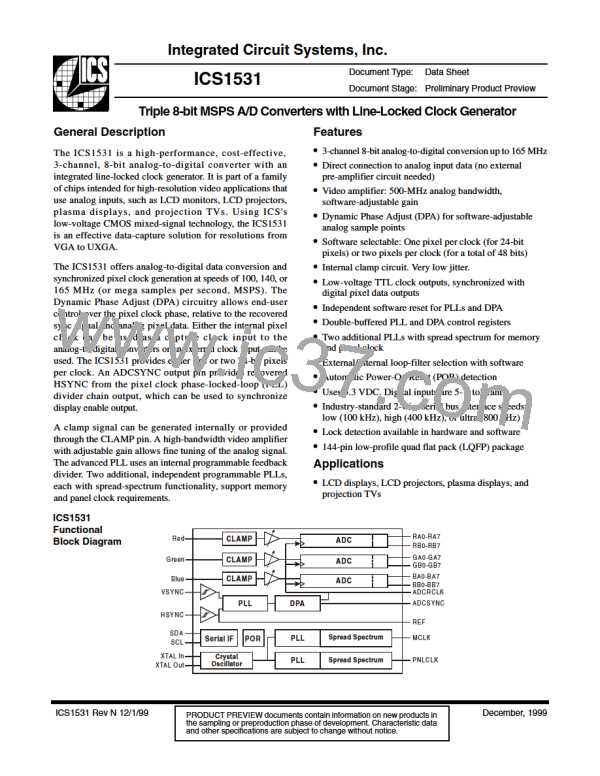
By using the internal 3-channel analog-to-digital converter (ADC), the ICS1531 internally provides the pixel
clock needed to synchronize data capture. The pixel clock can be further processed by the Dynamic Phase
Adjust. [For more information on the ADC, see Section 2.2.3, “Analog-to-Digital Circuits (Digitize RGB
Inputs)” and Figure 4-3.] For the pixel clock to appear on the CLK pin, the pixel clock output must be
enabled (Reg 06:6).
ICS1531 Rev N 12/1/99
December, 1999
Copyright © 1999, Integrated Circuit Systems, Inc.
All rights reserved.
6

 ICSI [ INTEGRATED CIRCUIT SOLUTION INC ]