ICS85301
2:1
DIFFERENTIAL-TO-LVPECL MULTIPLEXER
Integrated
Circuit
Systems, Inc.
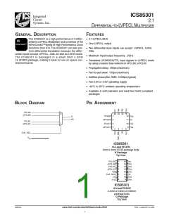
TABLE 1. PIN DESCRIPTIONS
Number
Name
Type
Description
1
PCLK0
Input
Input
Input
Input
Pulldown Non-inverting differential LVPECL clock input.
Pullup/
2
3
4
nPCLK0
PCLK1
Inverting differential LVPECL clock input. VCC/2 default when left floating.
Pulldown
Pulldown Non-inverting differential LVPECL clock input.
Pullup/
nPCLK1
Inverting differential LVPECL clock input. VCC/2 default when left floating.
Pulldown
5
VBB
nc
Output
Bias voltage.
No connect.
7, 16
Unused
Clock select input. When HIGH, selects PCLK1, nPCLK1 inputs.
Pulldown When LOW, selects PCLK0, nPCLK0 inputs.
LVCMOS / LVTTL interface levels.
6
CLK_SEL
Input
8, 13
9, 12, 14, 15
10, 11
VCC
VEE
Power
Power
Output
Positive supply pins.
Negative supply pins.
nQ, Q
Differential output pair. LVPECL interface levels.
NOTE: Pullup and Pulldown refer to internal input resistors. See Table 2, Pin Characteristics, for typical values.
TABLE 2. PIN CHARACTERISTICS
Symbol
CIN
Parameter
Test Conditions
Minimum
Typical
Maximum
Units
pF
Input Capacitance
Input Pullup Resistor
1
RPULLUP
37
37
kΩ
RPULLDOWN Input Pulldown Resistor
kΩ
TABLE 3. CONTROL INPUT FUNCTION TABLE
Input
Input Selected
PCLK
CLK_SEL
0
1
PCLK0, nPCLK0
PCLK1, nPCLK1
85301AK
www.icst.com/products/hiperclocks.html
REV.A JANUARY 16, 2006
2

 ICSI [ INTEGRATED CIRCUIT SOLUTION INC ]