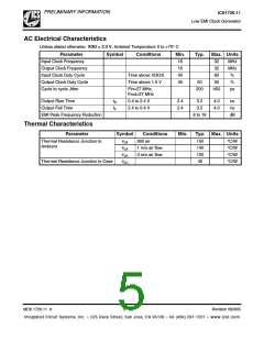
PRELIMINARY INFORMATION
ICS1726-11
Low EMI Clock Generator
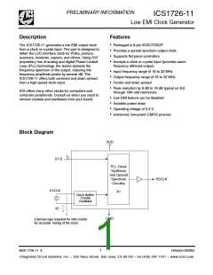
Pin Assignment
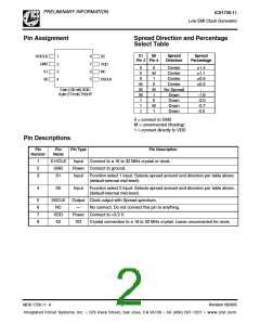
Spread Direction and Percentage
Select Table
S1
S0
Spread
Direction
Spread
Percentage
X1/ICLK
GND
S1
8
7
6
5
1
2
3
4
X2
Pin 3 Pin 4
VDD
NC
0
0
0
M
M
M
1
0
M
1
0
M
1
0
M
1
Center
Center
Center
Center
No Spread
Down
1.4
1.1
0.6
0.5
-
-1.6
-2.0
-0.7
-3.0
S0
SSCLK
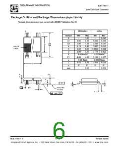
8 pin (150 mil) SOIC
8-pin (173 mil) TSSOP
Down
Down
Down
1
1
0 = connect to GND
M = unconnected (floating)
1 = connect directly to VDD
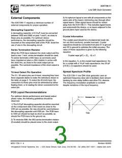
Pin Descriptions
Pin
Pin
Pin Type
Pin Description
Number
Name
1
2
3
X1/ICLK
GND
S1
Input
Connect to a 16 to 32 MHz crystal or clock.
Power Connect to ground.
Input
Function select 1 input. Selects spread amount and direction per table above.
(default-internal mid-level).
4
S0
Input
Function select 0 input. Selects spread amount and direction per table above.
(default-internal mid-level).
5
6
7
8
SSCLK
NC
Output Clock output with Spread spectrum.
No connect. Do not connect this pin to anything.
Power Connect to +3.3 V.
XO Crystal connection to a 16 to 32 MHz crystal. Leave unconnected for clock.
—
VDD
X2
MDS 1726-11 A
2
Revision 092905
Integrated Circuit Systems, Inc. ● 525 Race Street, San Jose, CA 95126 ● tel (408) 297-1201 ● www.icst.com

 ICSI [ INTEGRATED CIRCUIT SOLUTION INC ]